
Finally some success!!! I was able to successfully etch a PCB this weekend. I followed many different tutorials (which you can find by asking Google) and this how I did it.
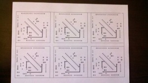
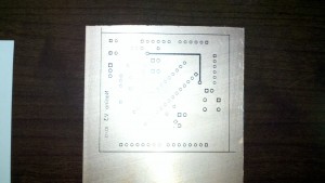
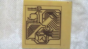
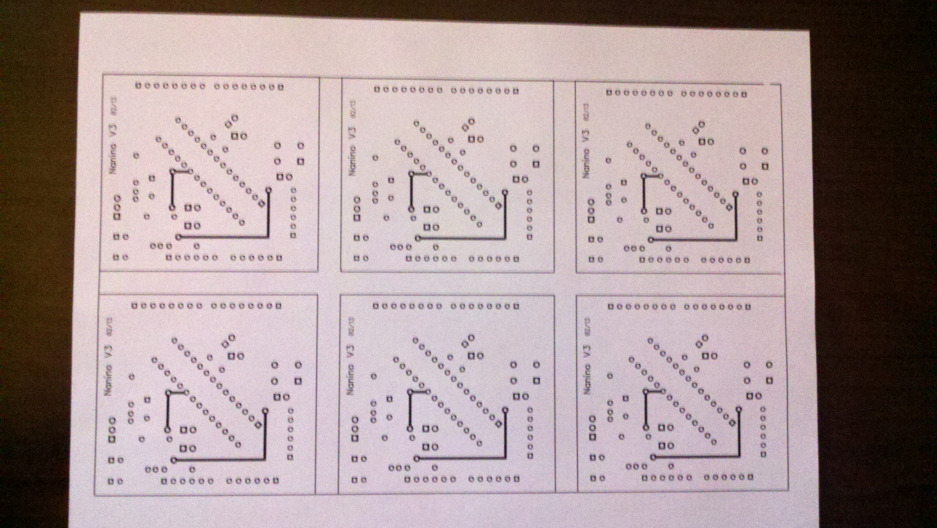
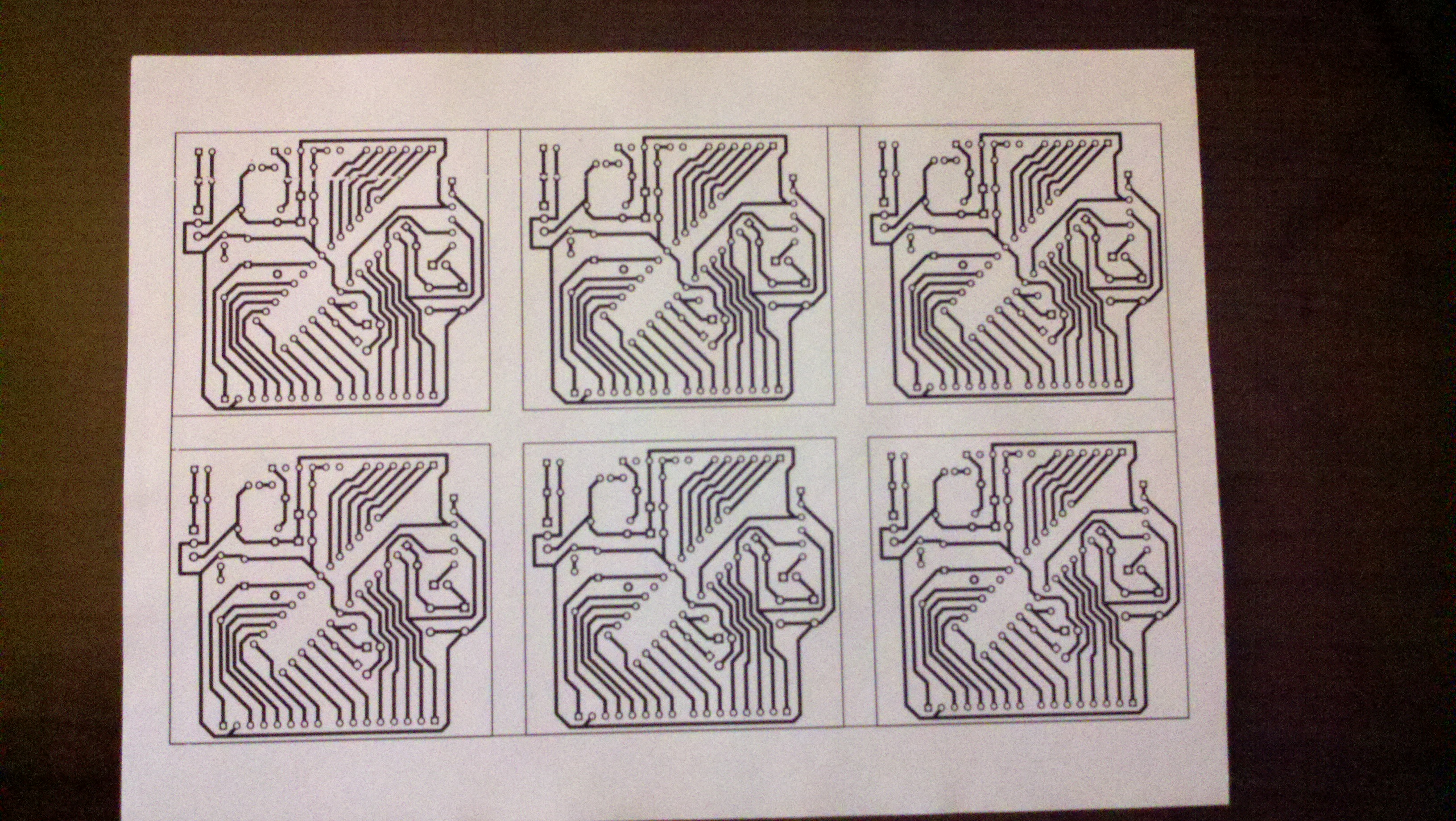
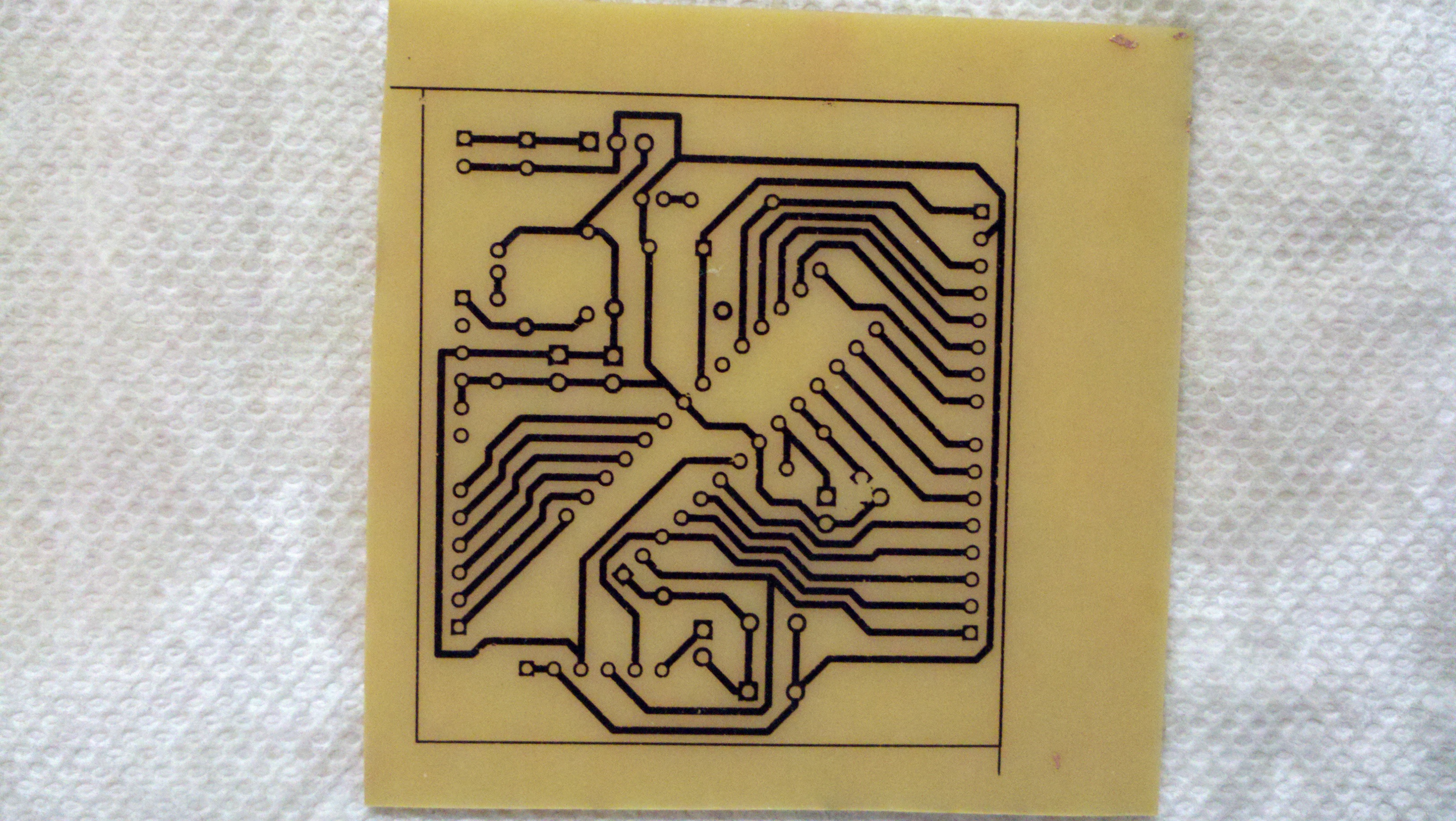
- Printing the schematic.
- I purchased Toner Transfer Paper http://www.amazon.com/Toner-Transfer-Electronic-Prototype-Sheets/dp/B00B0ZDXB2/ref=sr_1_1?ie=UTF8&qid=1364912557&sr=8-1&keywords=toner+transfer+paper
- I used DipTrace http://www.diptrace.com/ to print the schematic
- Several printers did NOT work. I think that you may have to use a black and white printer only
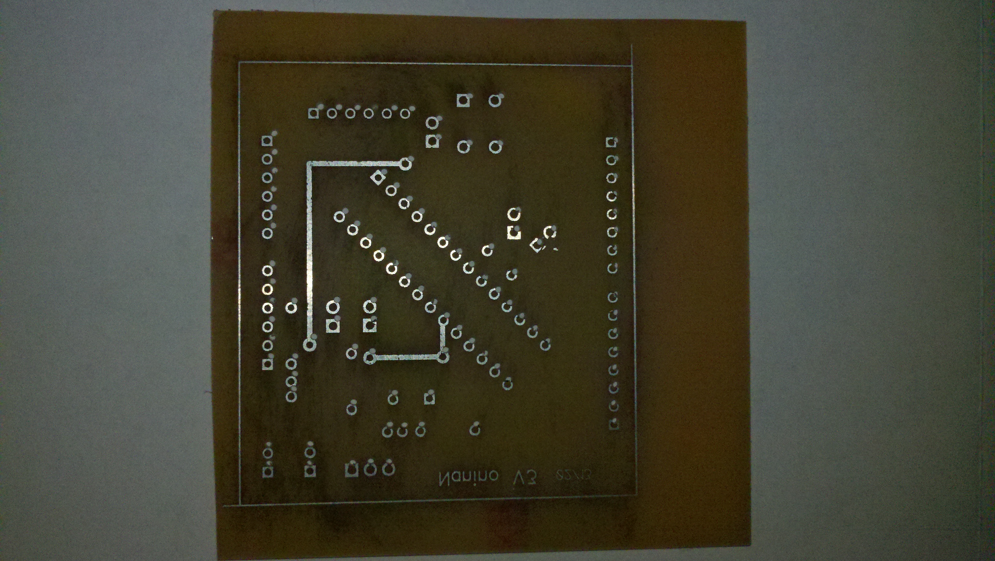
Top
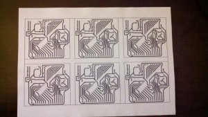
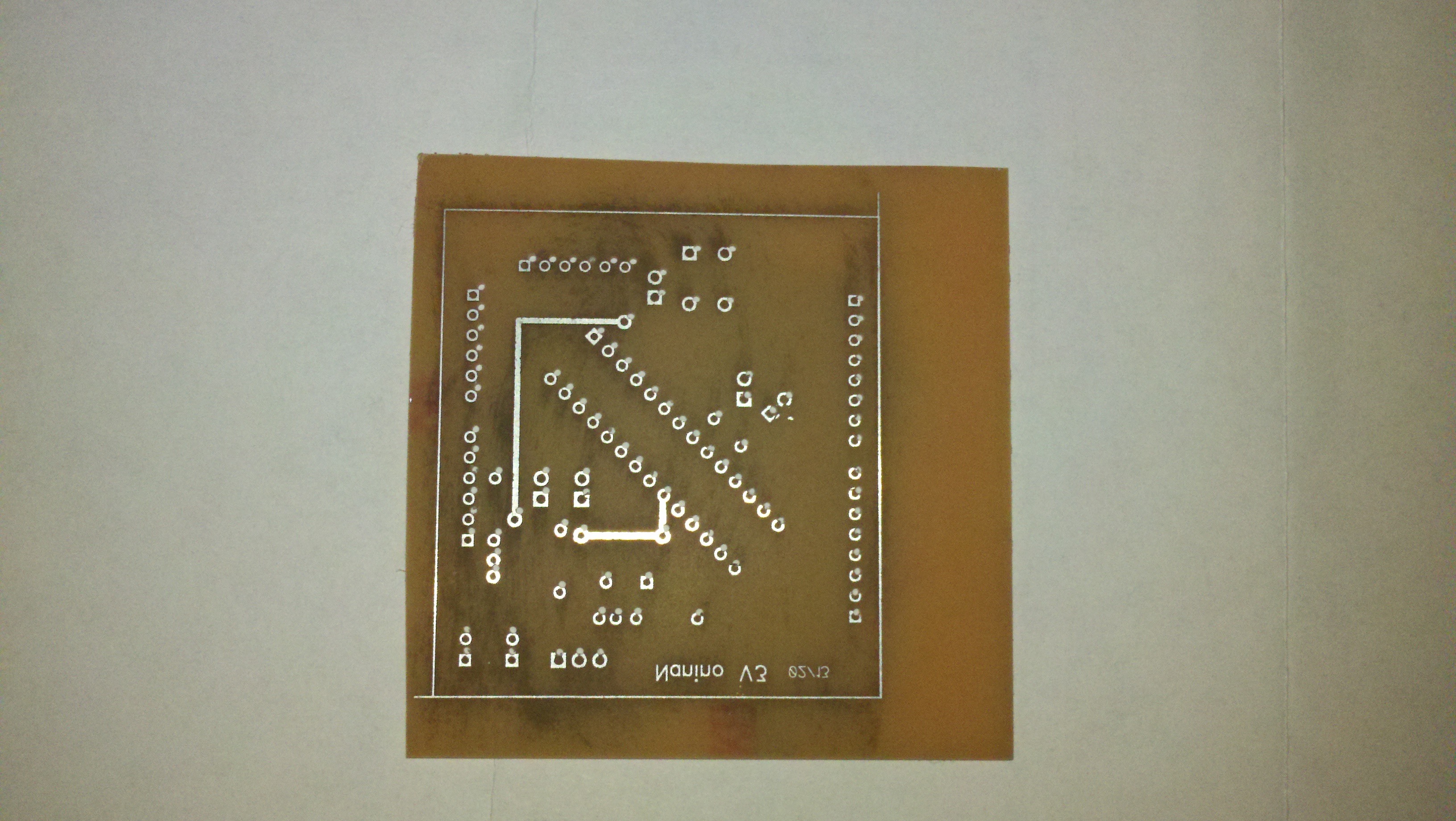
Bottom
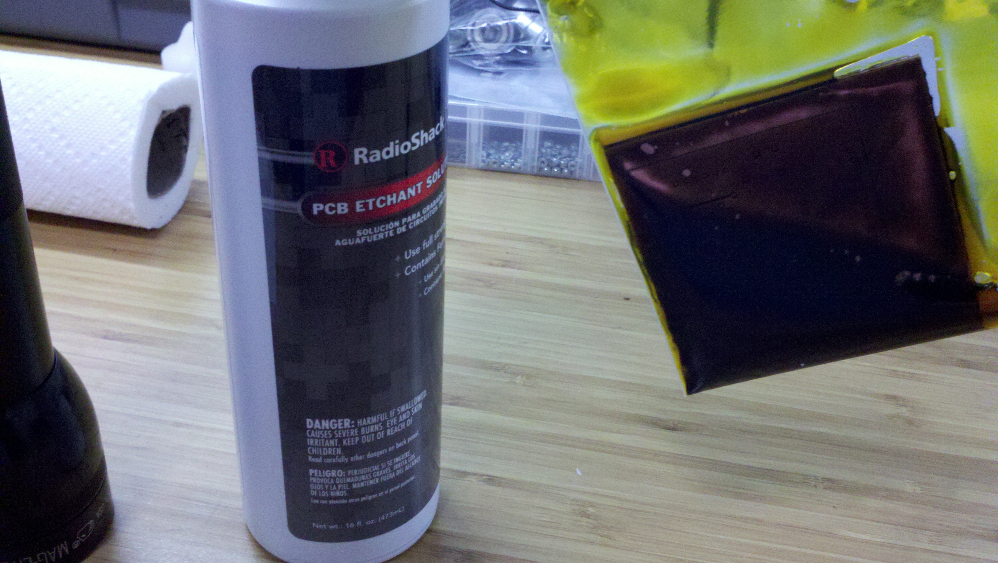
- I got some copper clad board http://www.radioshack.com/product/index.jsp?productId=2102495. And cut it to approximately the right size for the PCB that I was making. In the future I don’t think that I will cut the board until after I do the transfer. This should reduce the waste board.
- I then thoroughly cleaned the board using acetone and paper towels making sure not to leave fingerprints on the board once cleaned
- Next I cut the schematics (top and bottom) and taped two sides together to make a “pocket” for the copper clad board. In retrospect this did not align the two sides correctly. I think this technique will work but I need to use a spacer made from scrap pcb so that the alignment is correct (see picks below)
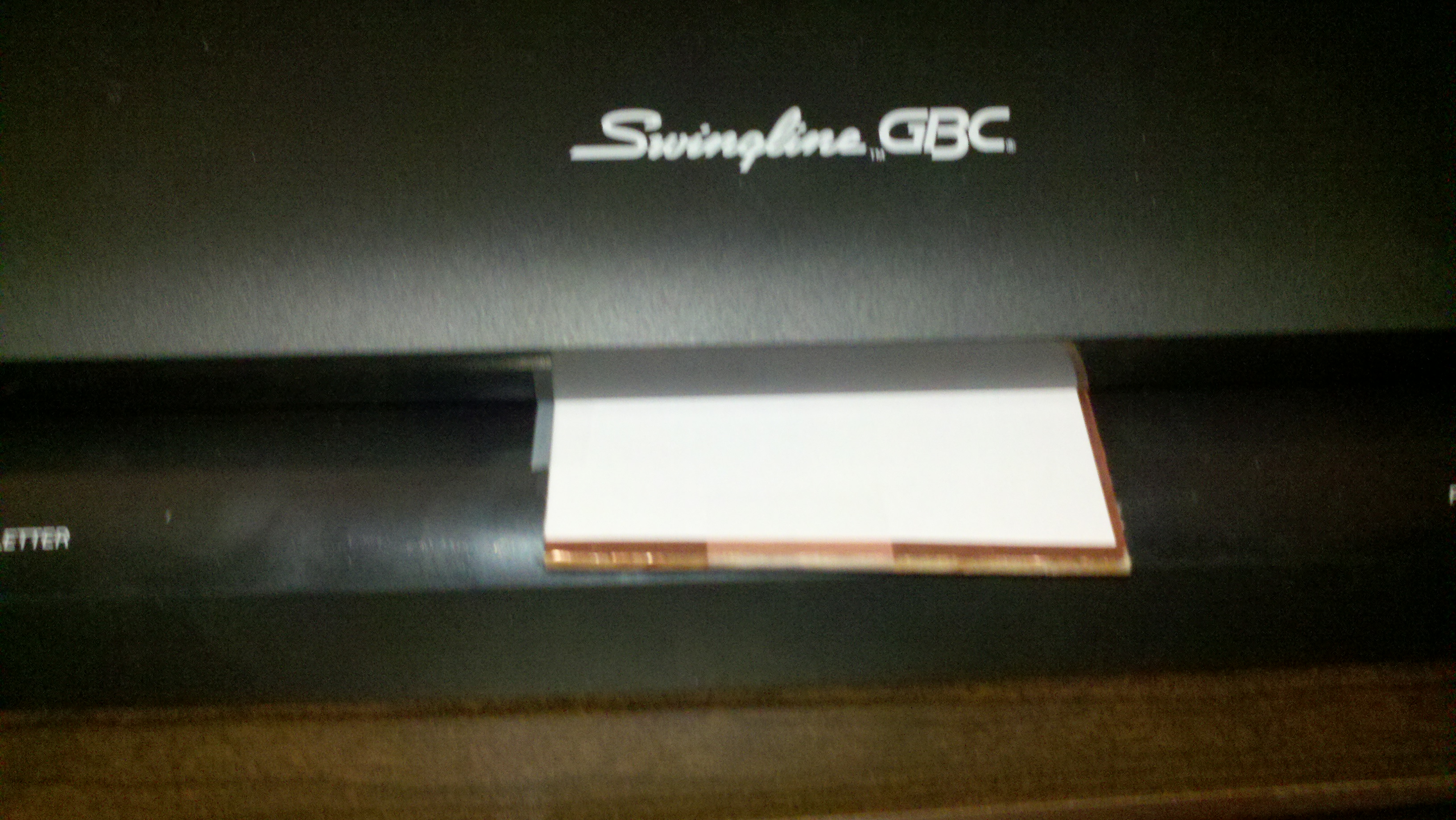
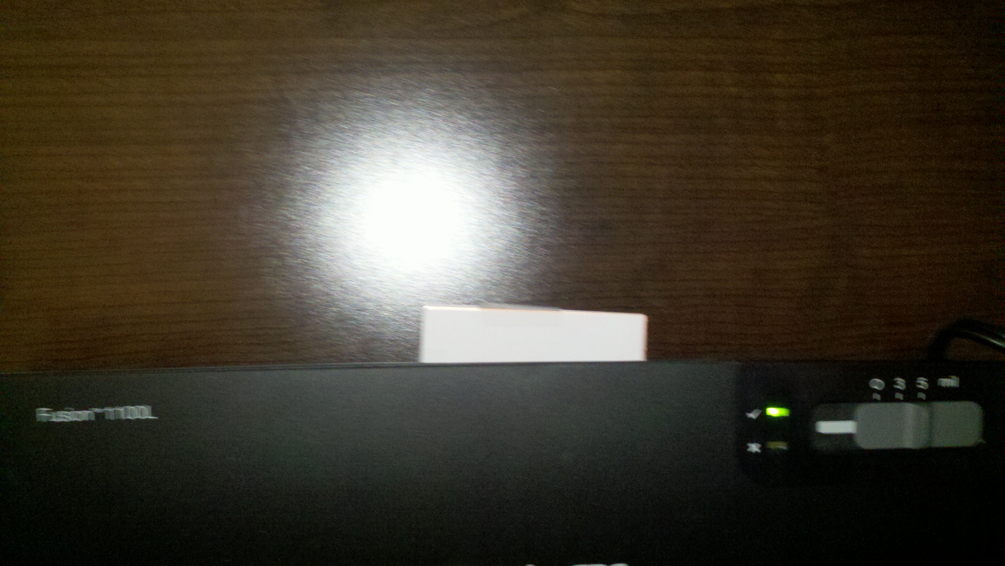
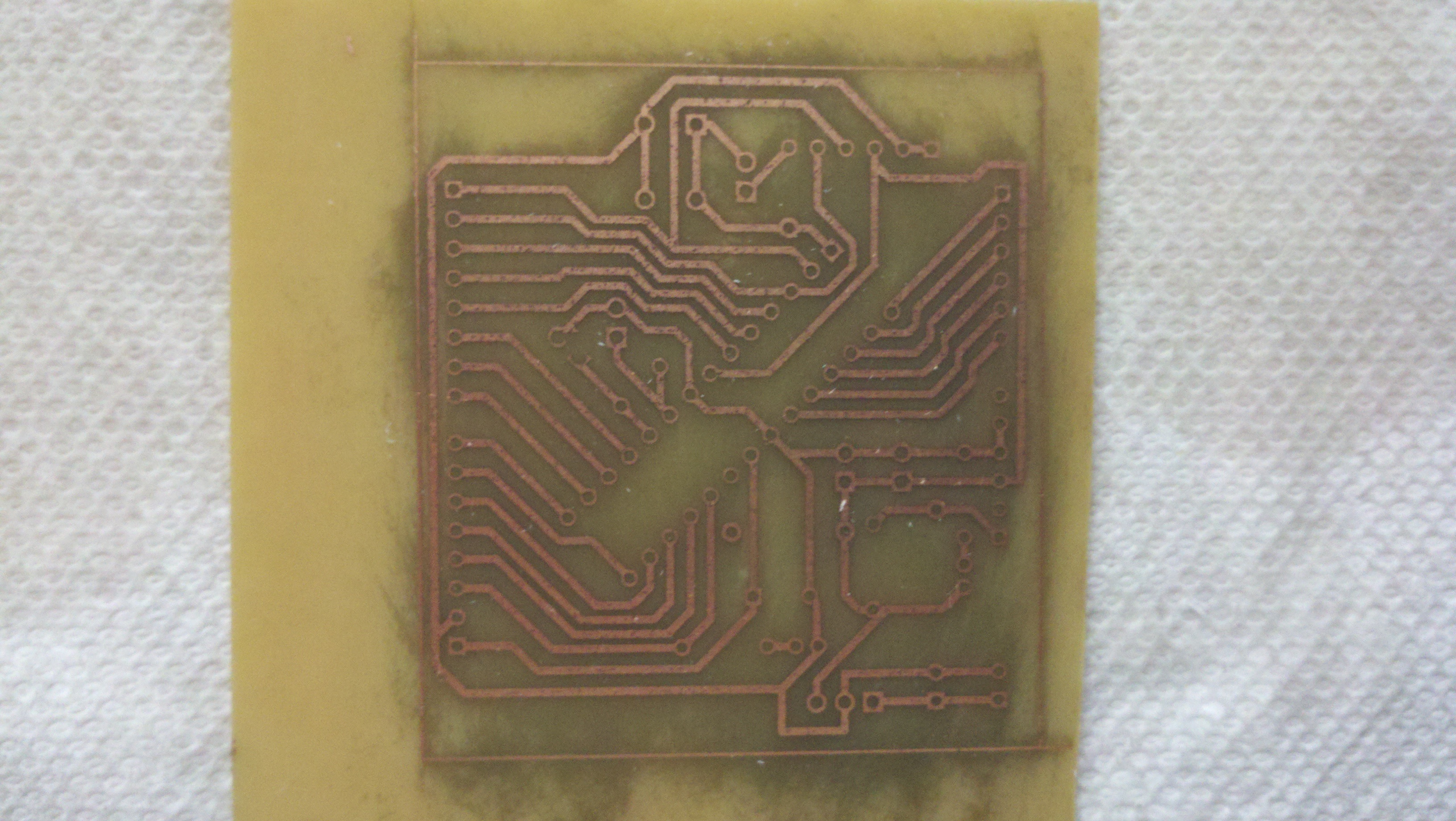
- I place the PCB into the pocket and ran the whole thing through a laminator http://www.amazon.com/Swingline-Fusion-Laminator-Warm-Up-1703074/dp/B009FFYIJA. I didn’t really know how many times to run it through so I ran it through about 15 times.

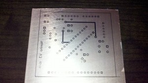
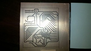
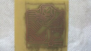
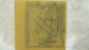
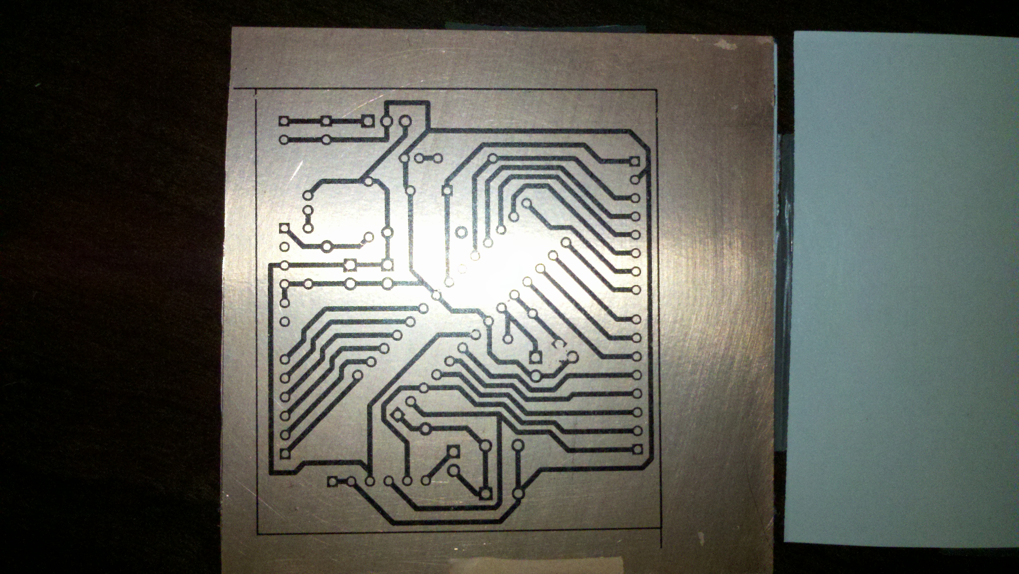
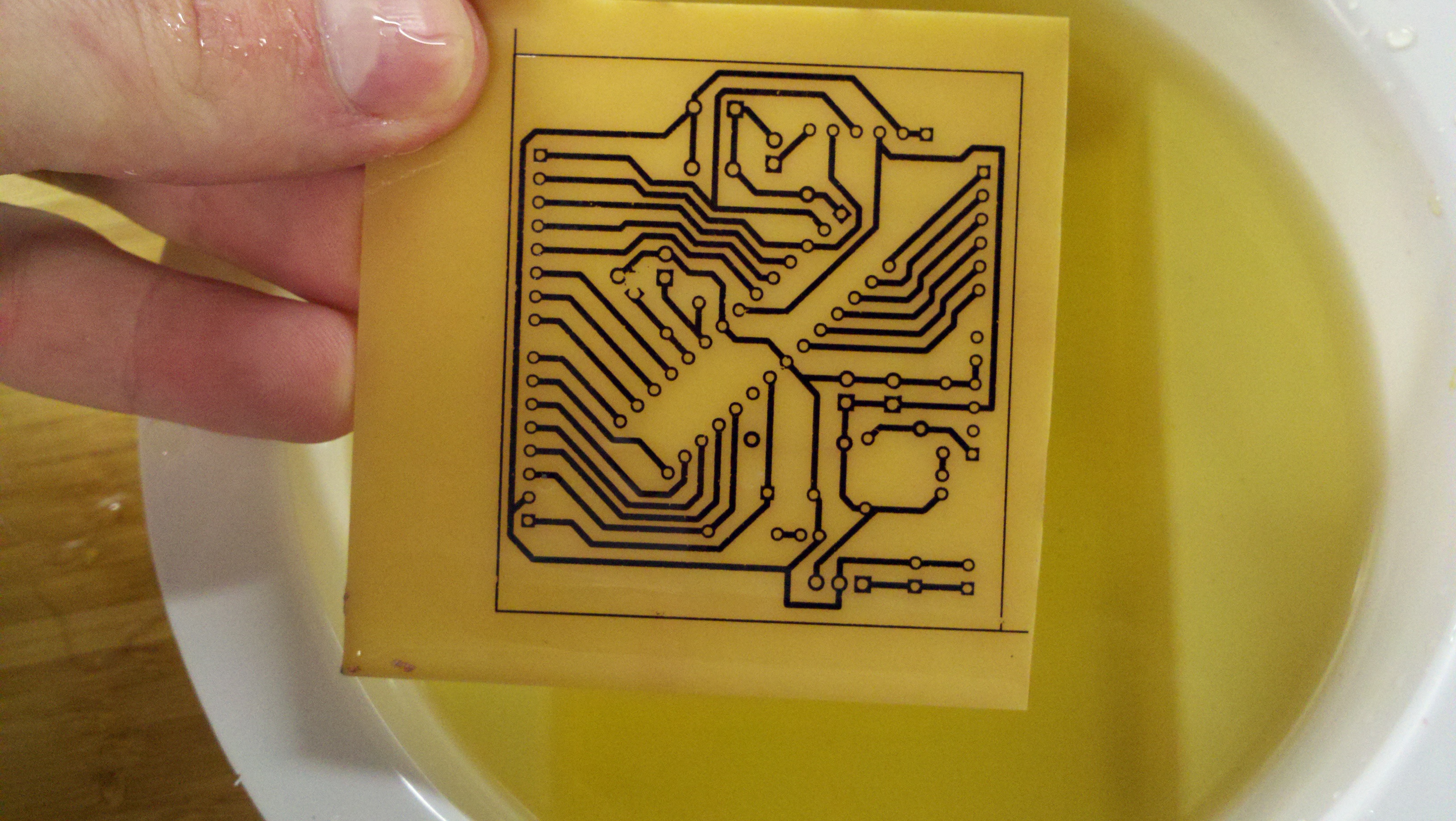
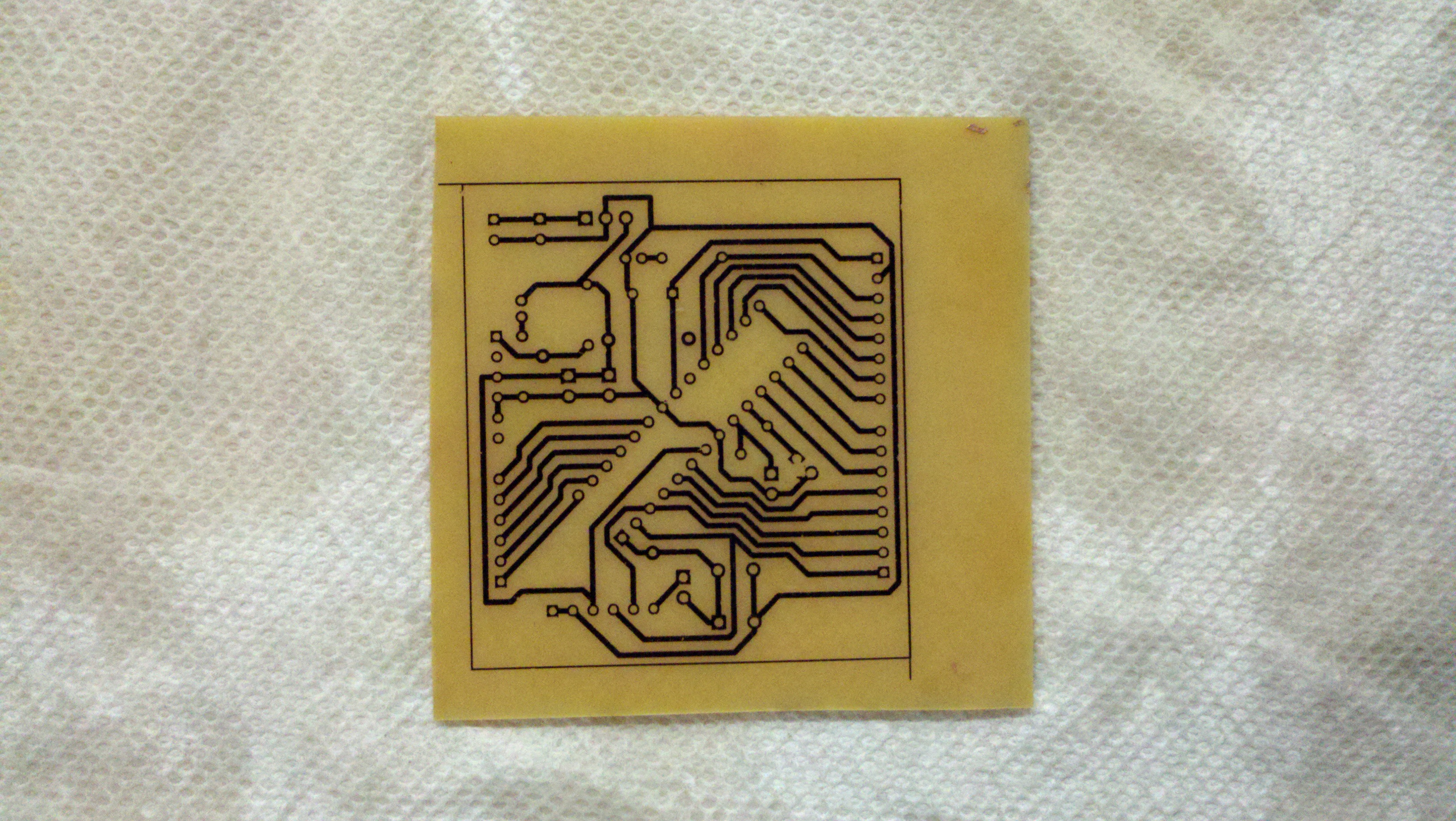
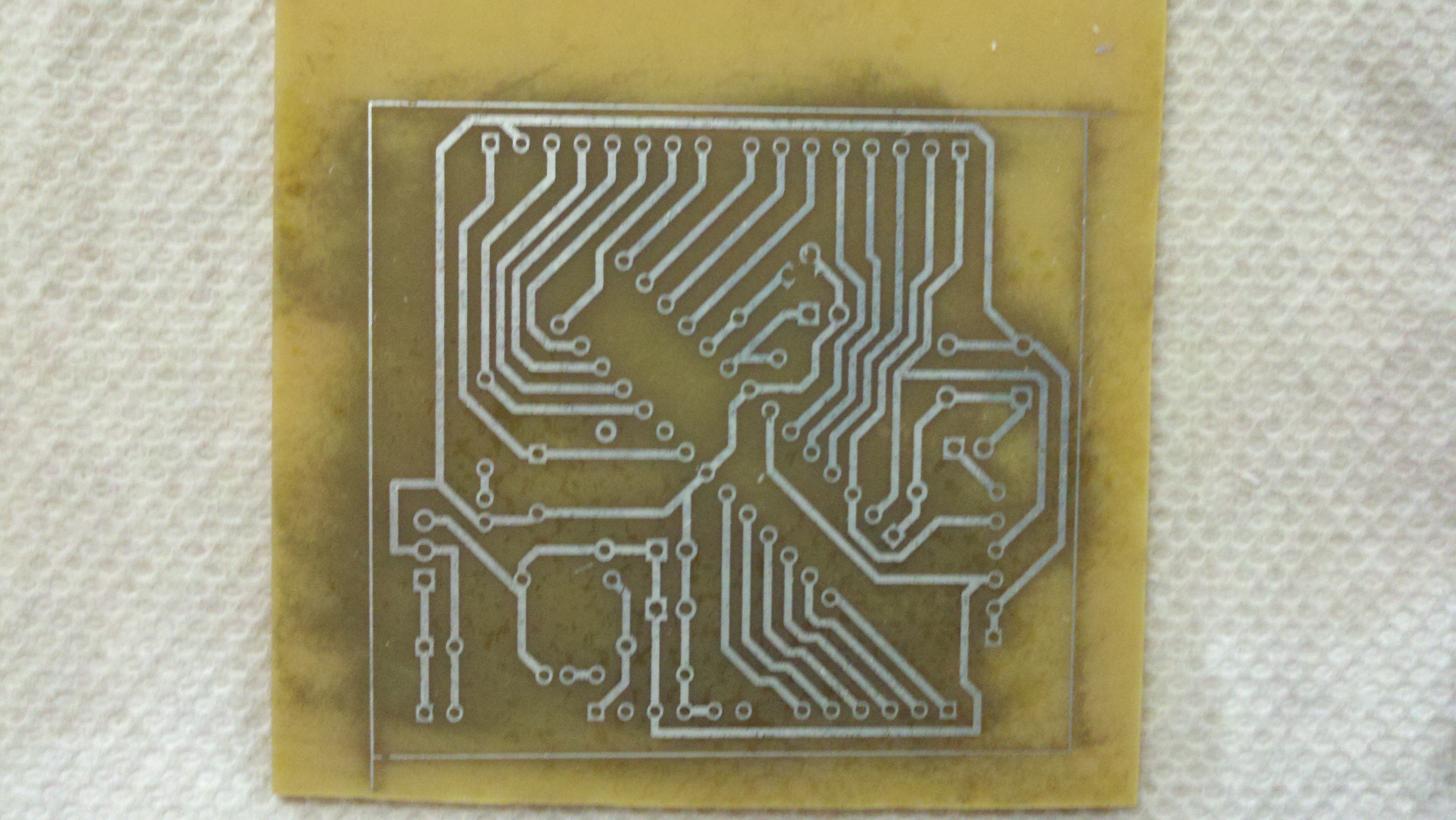
- Surprisingly I did not have to soak the paper it simply lifted away and left the toner on the paper. I am thoroughly impressed on the sharpness of the toner on the PCB.

All the toner transfered
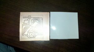
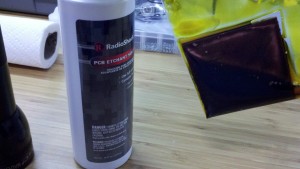
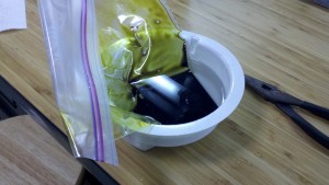
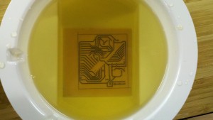
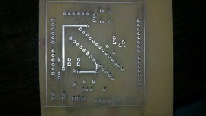
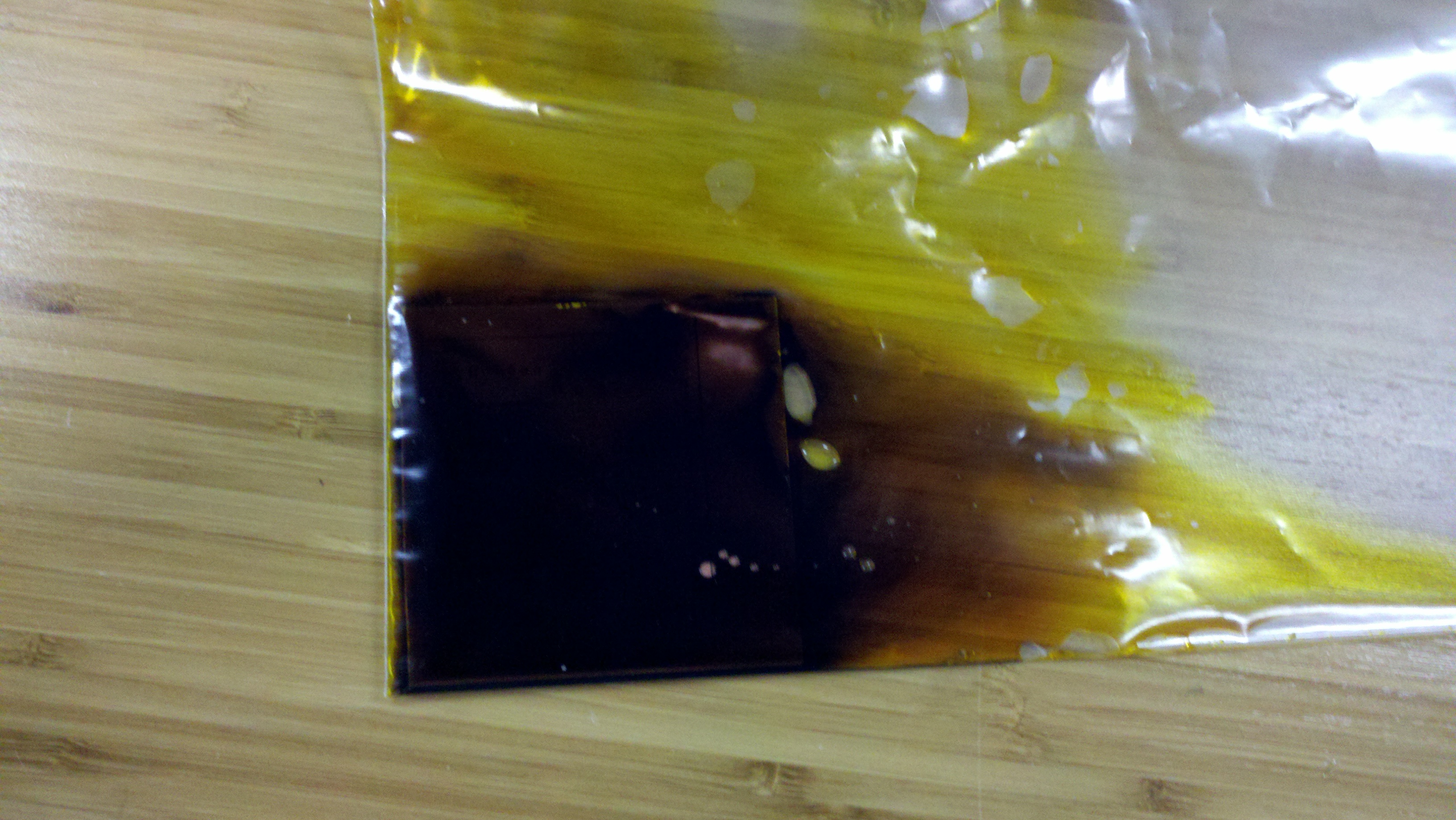
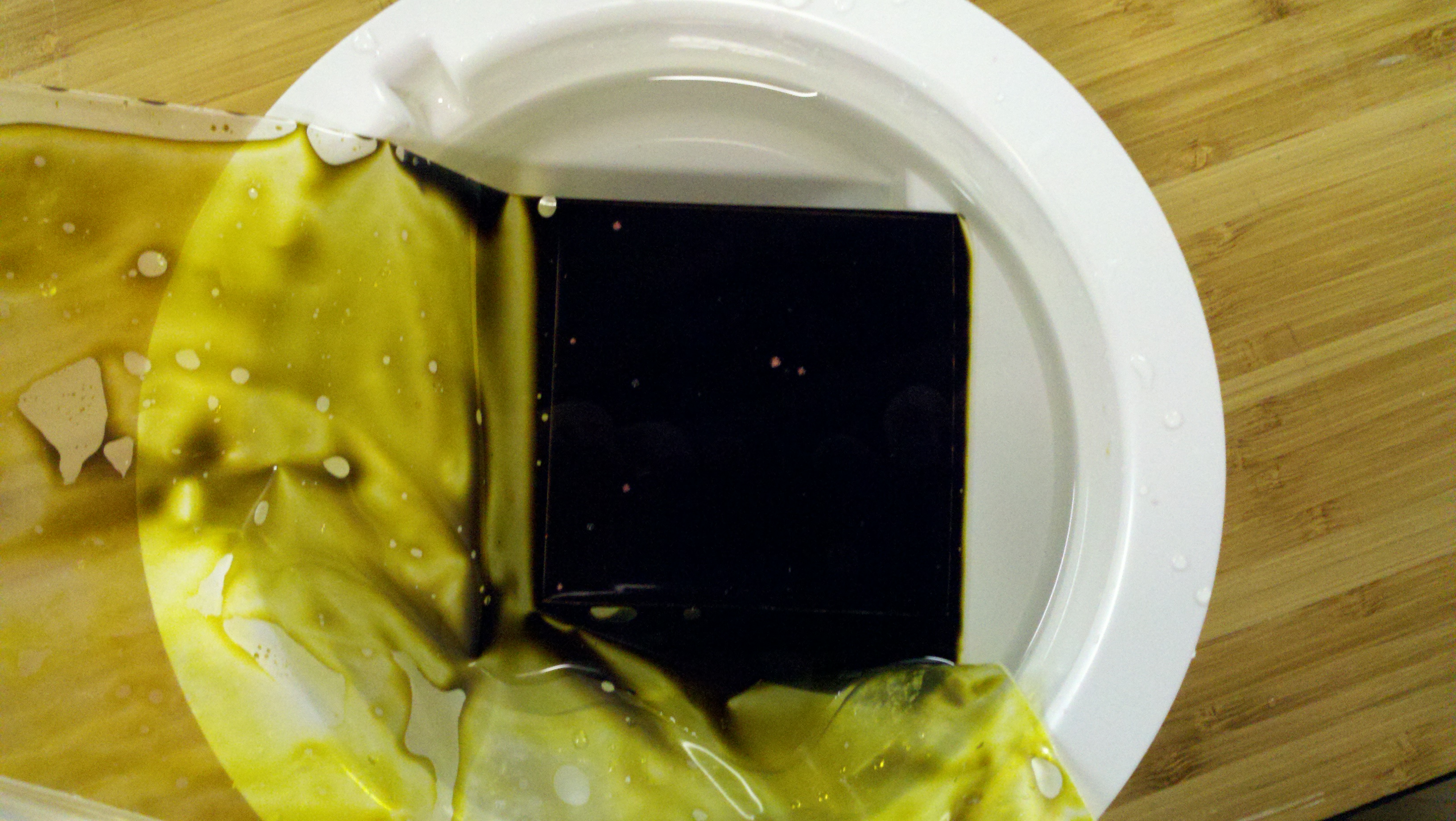
- Next I placed the PCB into a zip lock bag and poured in some ferric chloride http://www.radioshack.com/product/index.jsp?productId=2102868. I then place the zip lock into a tub of hot (from the tap) water. This took longer than I expected. I estimate that it took about 30-35 mins. Although I did remove the board twice and rinsed it to check the progress.


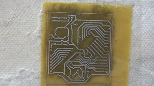
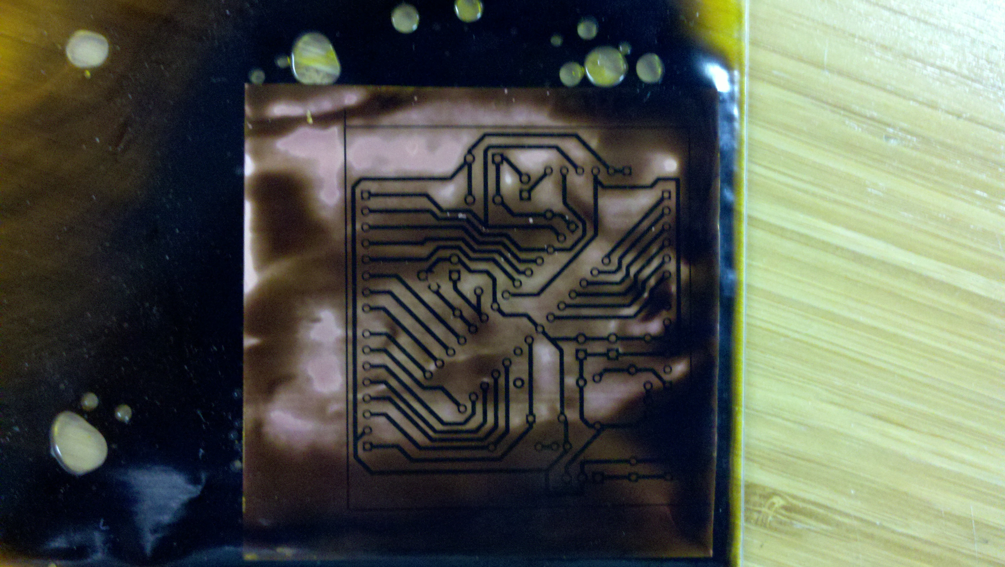
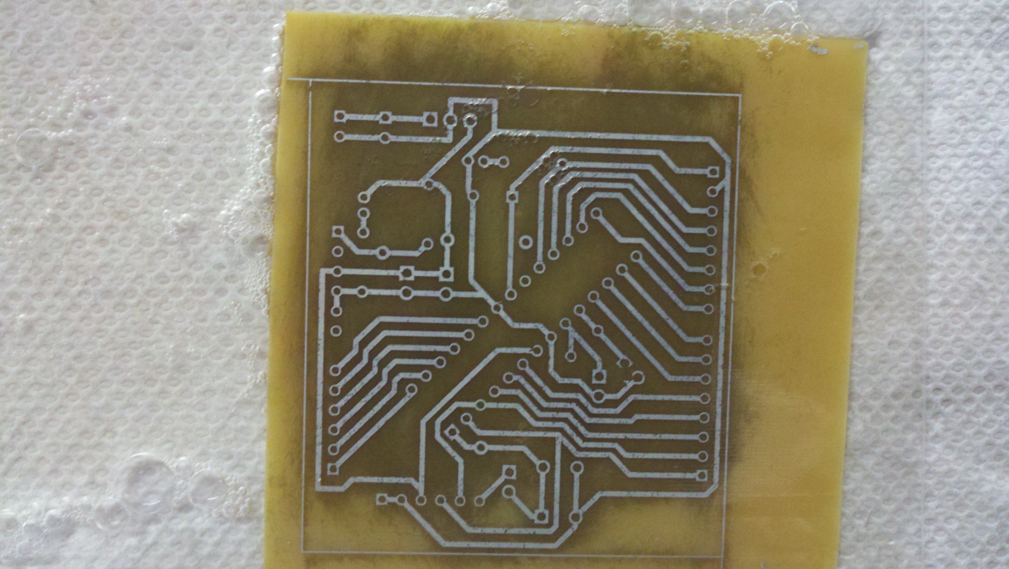
- Once it was fully etched I remove it an rinsed it in water and dried it with paper towel.


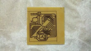
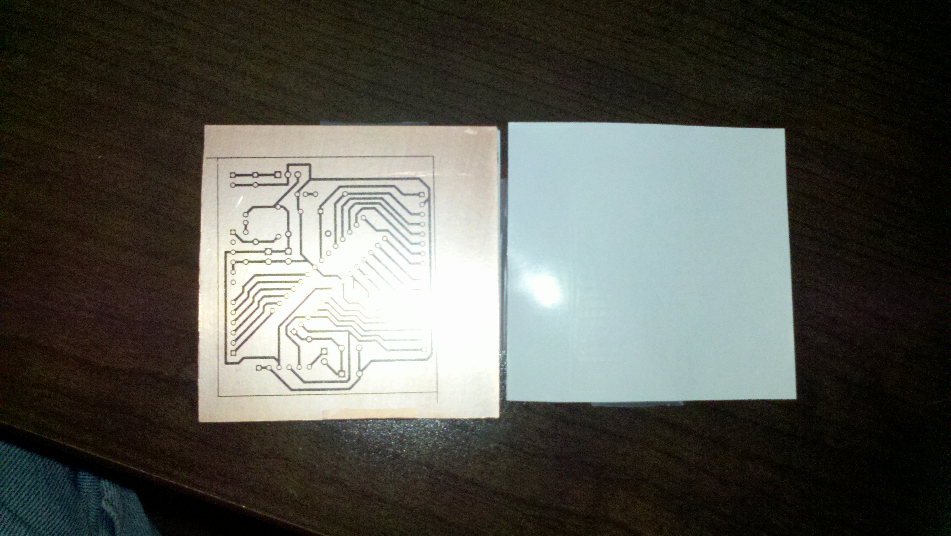
- Next I used Acetone to remove the toner which is the black stains you now see.
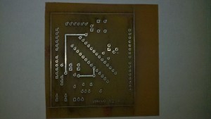
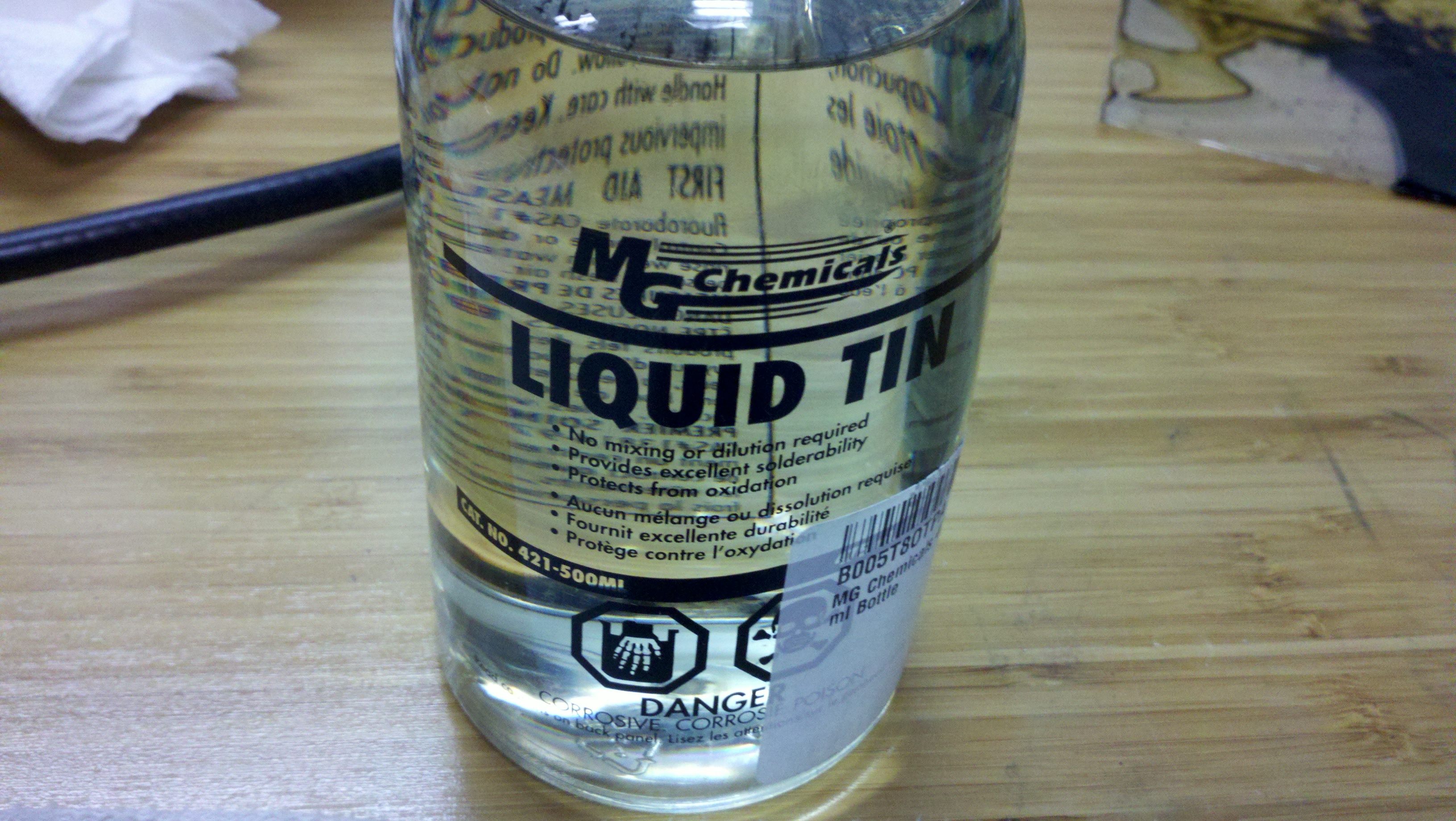
- Then I placed the PCB into another zip lock and poured in some Liquid Tin http://www.amazon.com/dp/B005T8PE4A/ref=biss_dp_t_asn. This only took about 3 mins. And when it was done I rinsed in water again. I also carefully poured the tin solution back into the bottle when I was done to reuse it later.

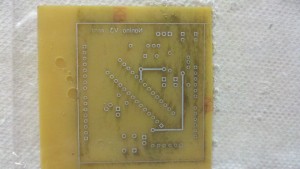

- Finally I used a Dremel Drill Press http://www.amazon.com/Dremel-220-01-Rotary-Tool-Station/dp/B00068P48O/ref=sr_1_1?ie=UTF8&qid=1364914163&sr=8-1&keywords=dremel+drill+press and a #65 (.035) http://www.amazon.com/gp/product/B000TY190C/ref=oh_details_o00_s01_i00?ie=UTF8&psc=1 drill to dill all the holes. Used http://www.amazon.com/gp/product/B0000DD2N3/ref=oh_details_o00_s01_i03?ie=UTF8&psc=1 also to hold the tiny drill.


This was the first time I did this so I do have some lessons learned:
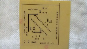
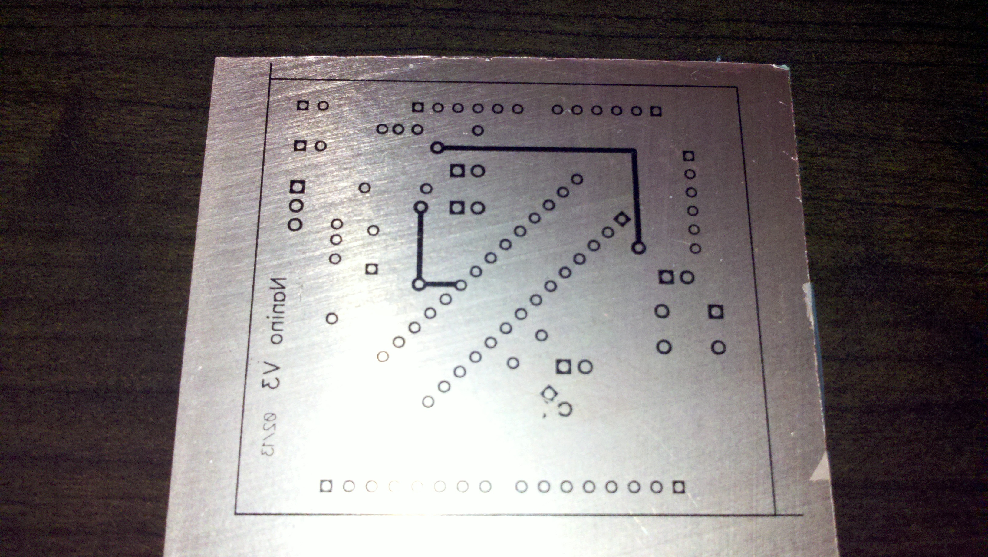
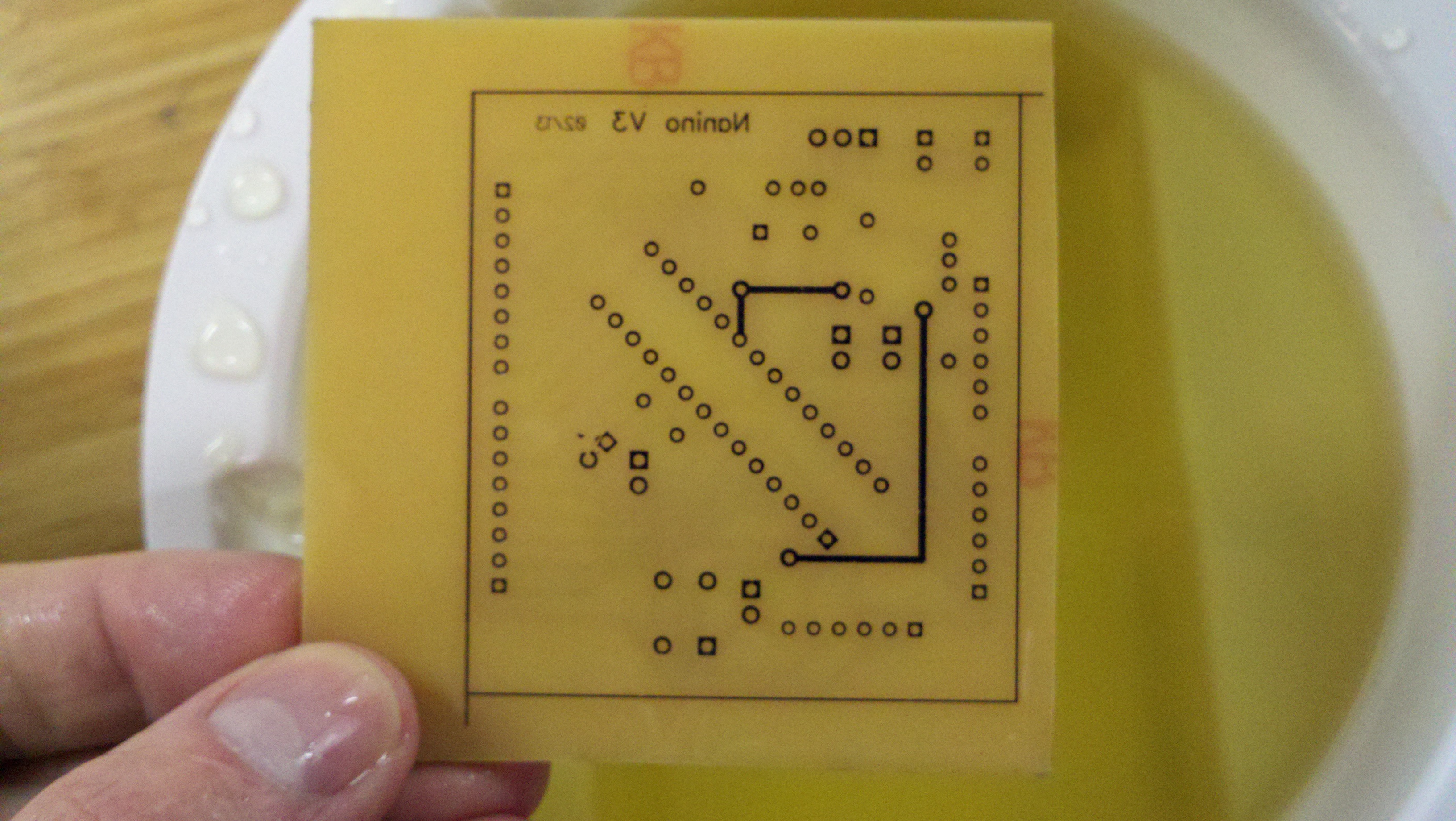
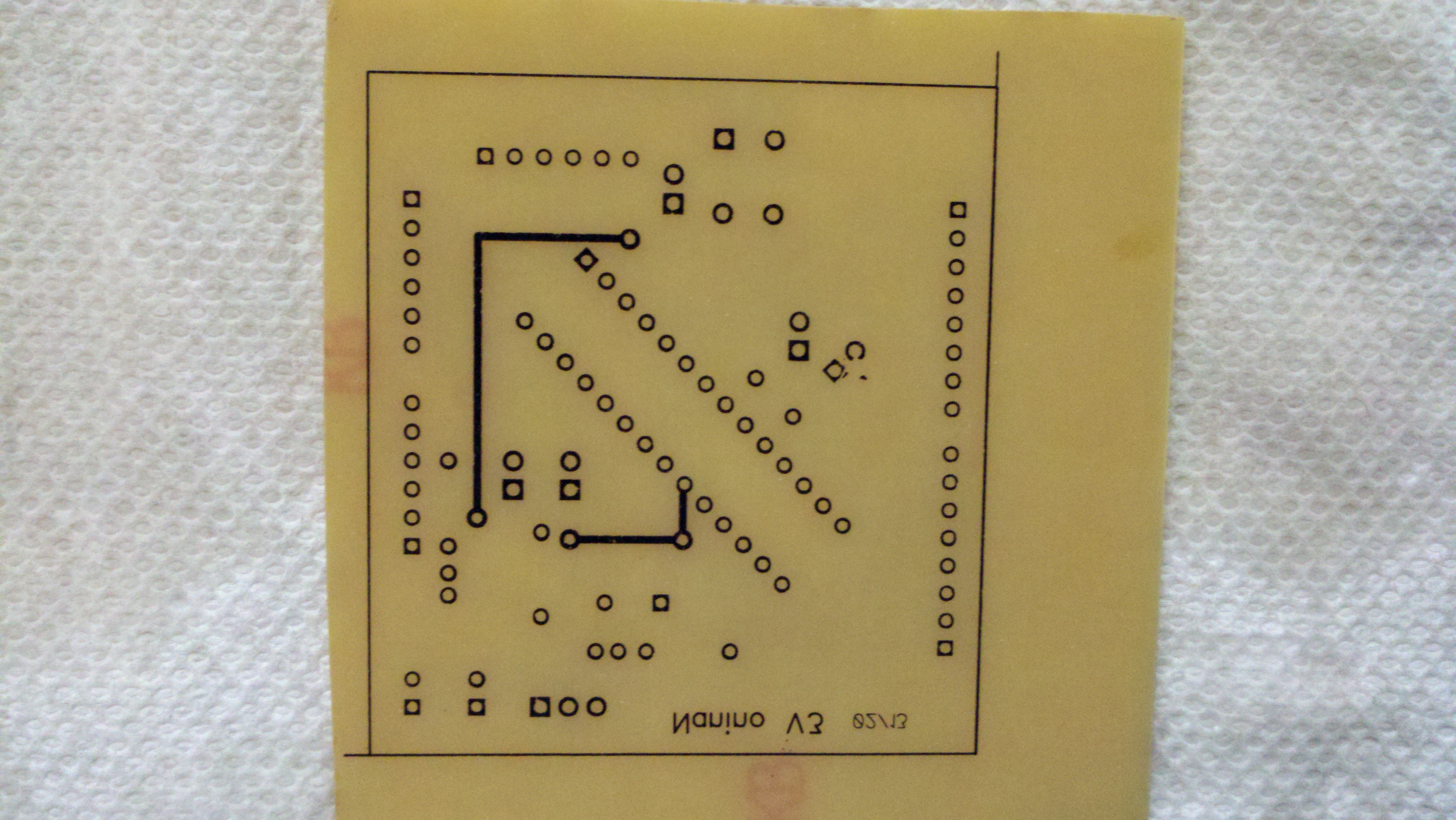
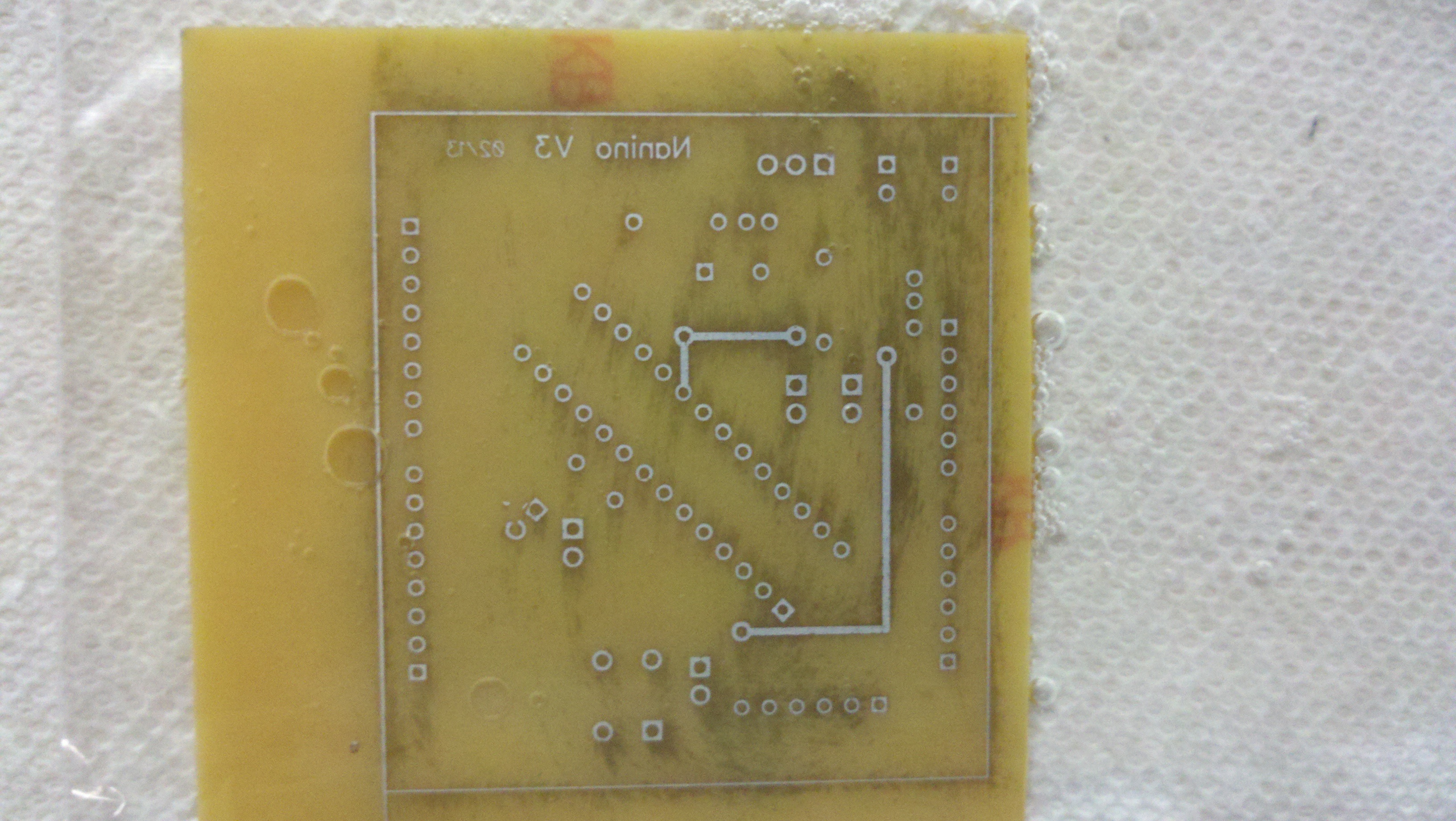
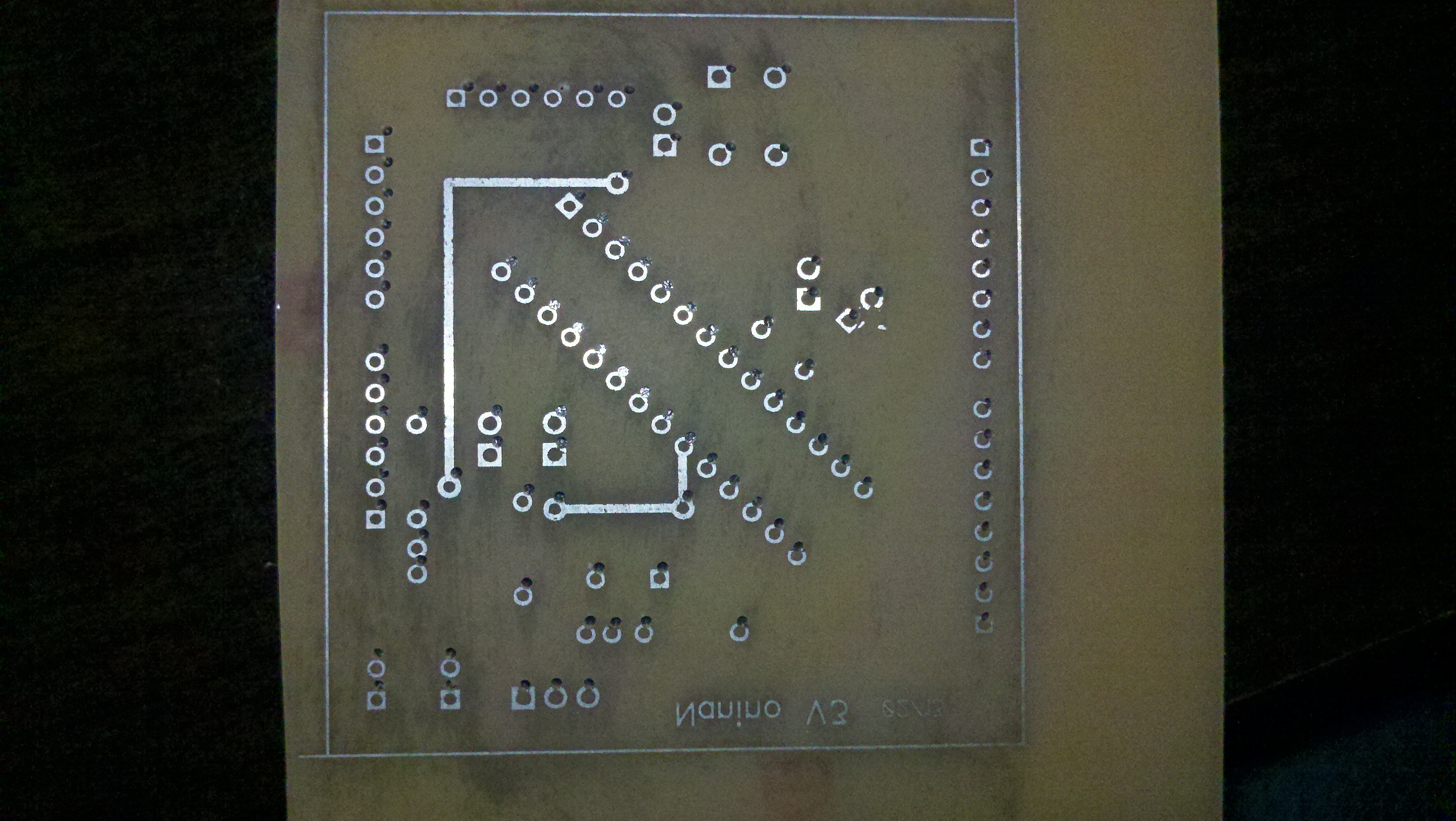
- When I printed the schematic I mirrored the bottom side of the PCB. This is necessary to match the top and bottom. The problem is that put the name of the board and date on the top of the board (copper pour). This made the words mirrored. If I had mirrored the top and not the bottom the words would have been correct. I will do this in the future.
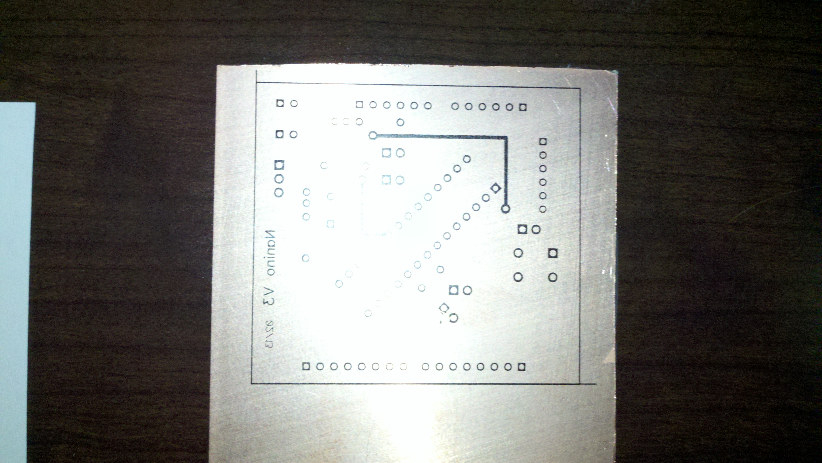
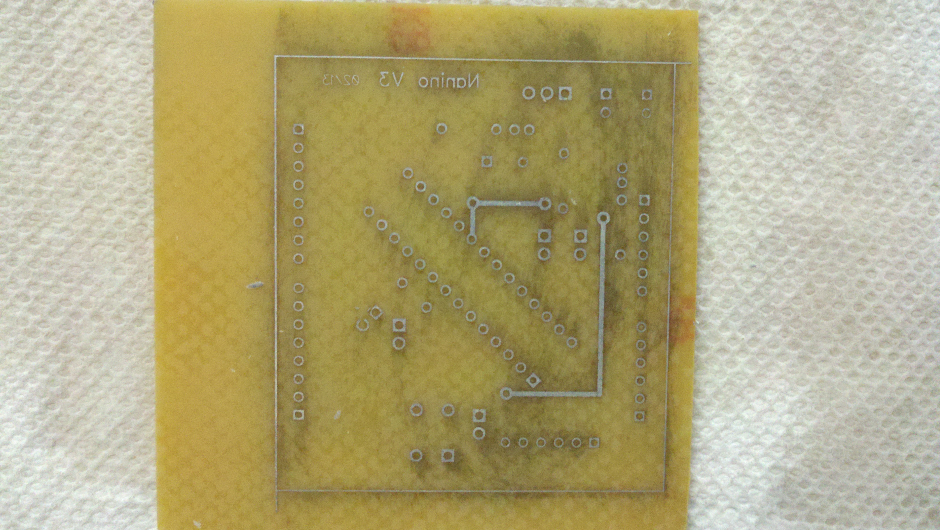
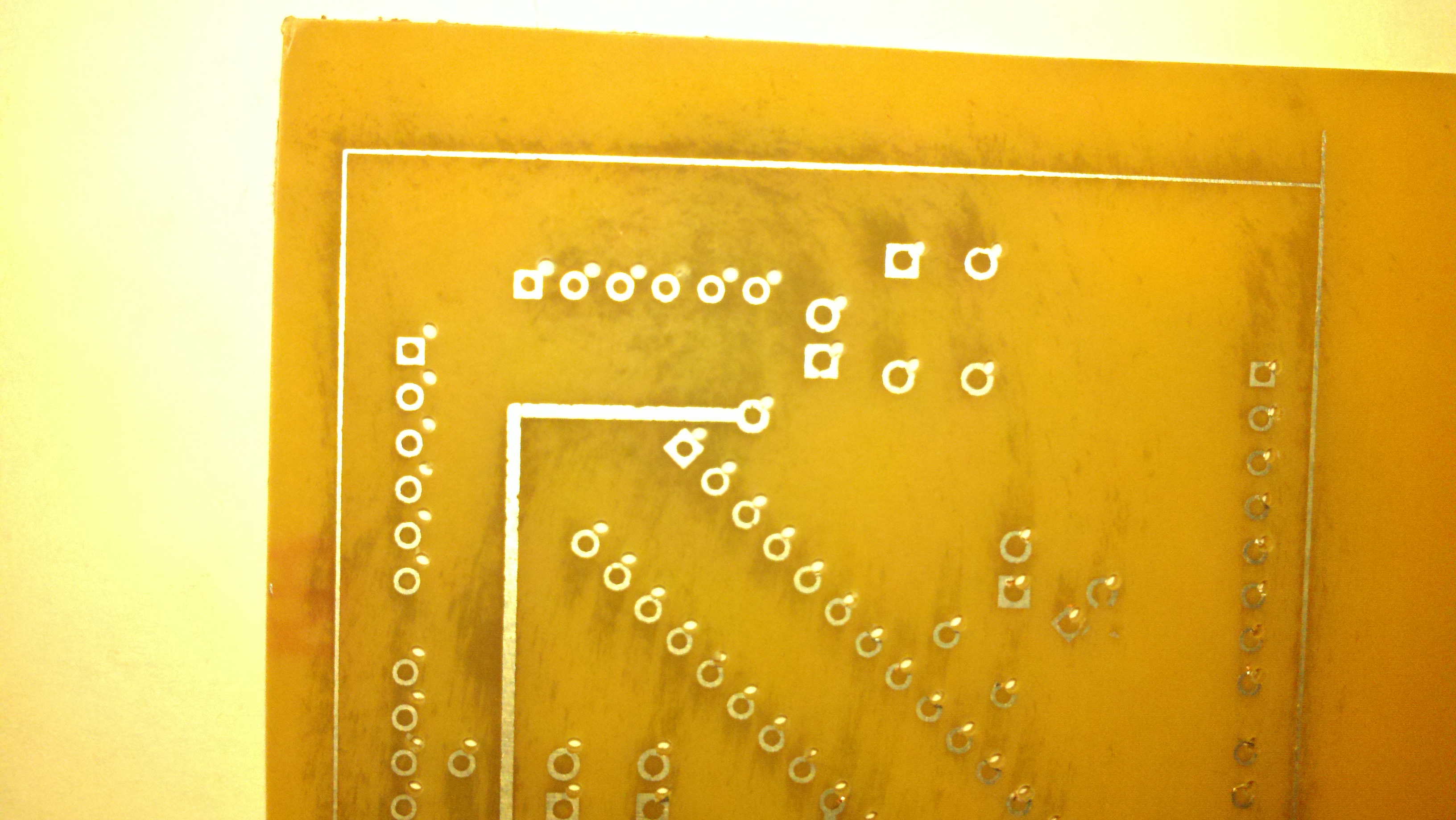
- The top and bottom alignment we off significantly. This is apparently the hardest thing in the whole process to do. I think I will try using a spacer out of scrap PCB when I make the pocket. If this does not work I may consider drilling a hole or two to match the top and bottom.
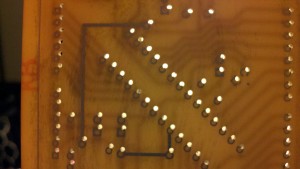
Close up of misalignment
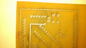
Close up of misalignment

Final thoughts:
Ultimately I had fun doing this which was the whole point. This was a bit more challenging that I had previously though (as my previous posts indicated) and I learned quite a lot. I will not use this first board since the top and bottom alignment is off but, I will etch another just like it (with improvements) and assemble it. I have passed along this board to a friend and he is going to try soldering legs to it to see how it behaves.