I did another attempt at etching the same PCB from the previous posts. I did a few things differently this time and got different results some good some bad.
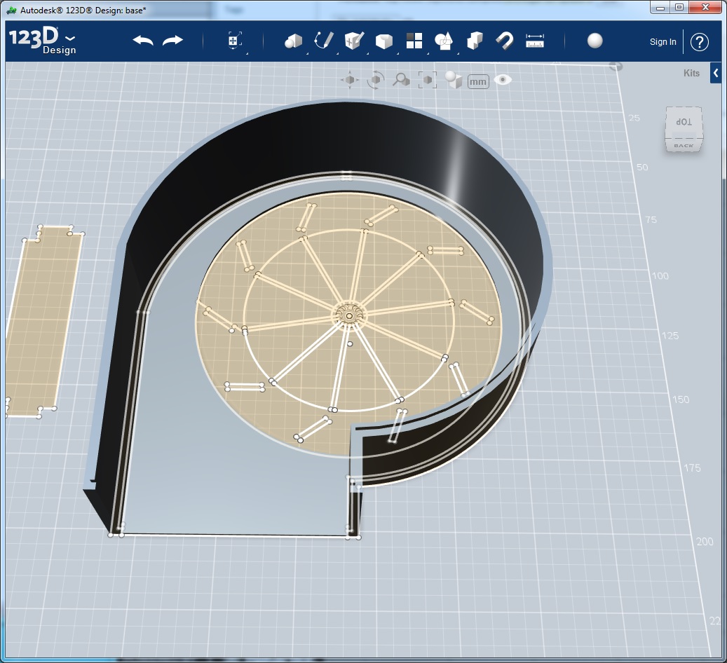
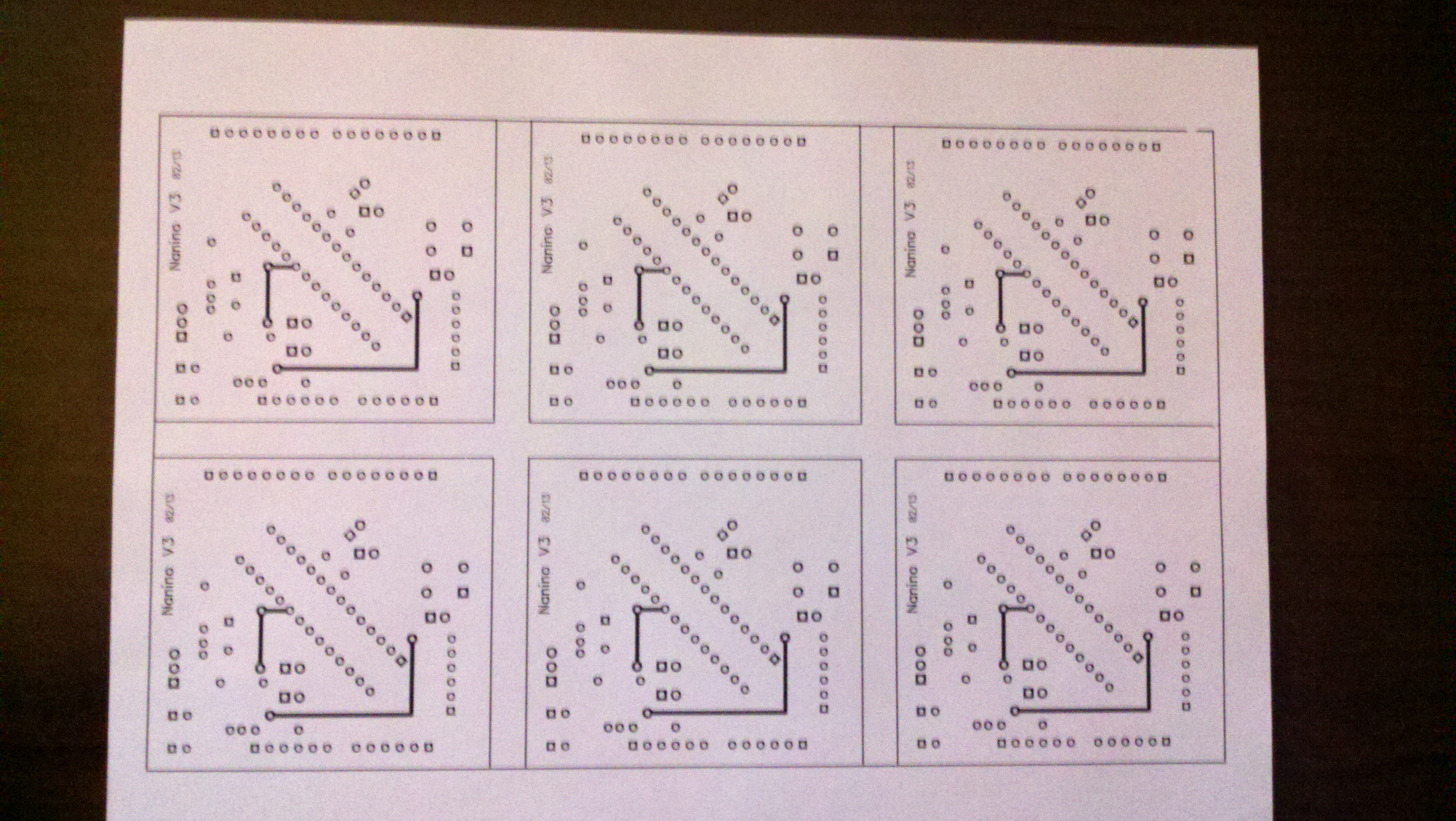
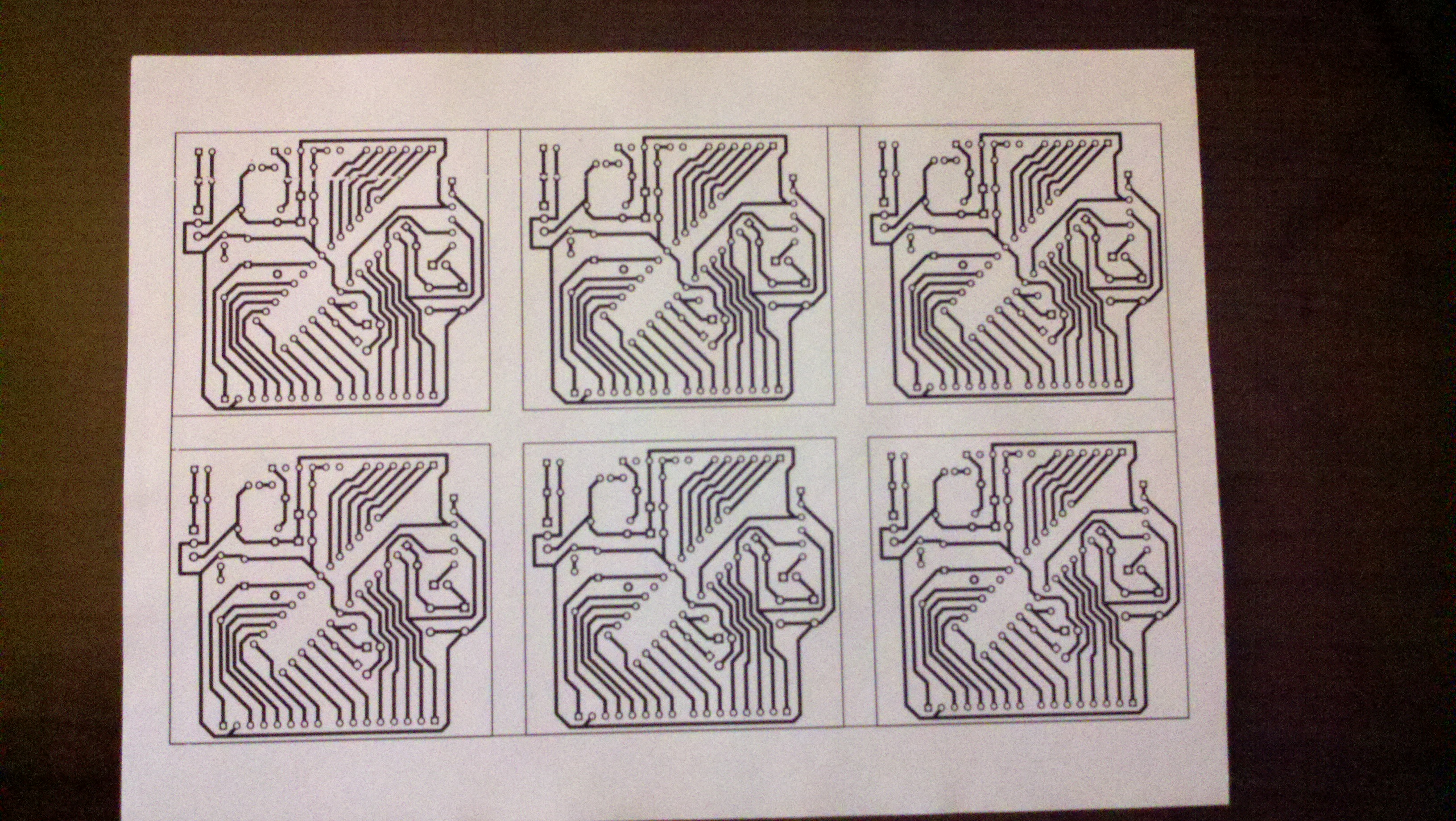
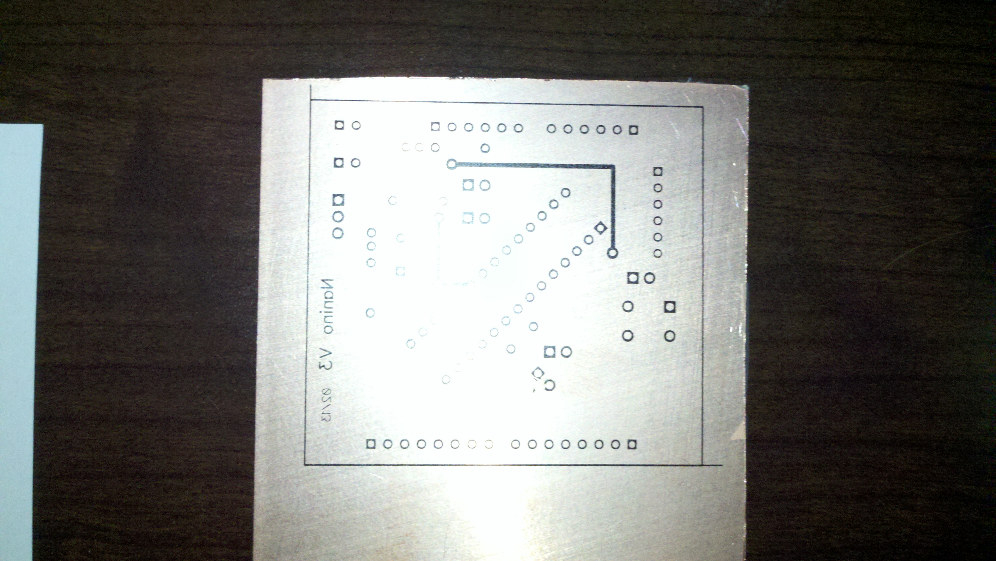
First I reworked the schematics. I increased the pad size of all holes to .075. When soldering some test legs to the previous etching I did we found that the pads detached from the board. Hopefully the larger pad will prevent this. Also I did a copper pour over the entire board to reduce the amount of etching that needs to take place. I did this mostly to save on enchant but it also seem like a good idea. Also as I found from the previous attempt that when printing on the transfer paper the top, which has the name of the board and version, should be mirrored when printed (instead of mirroring the bottom). That way when it is transferred it will read correctly. I also added registration marks to the print for aligning the top and bottom.
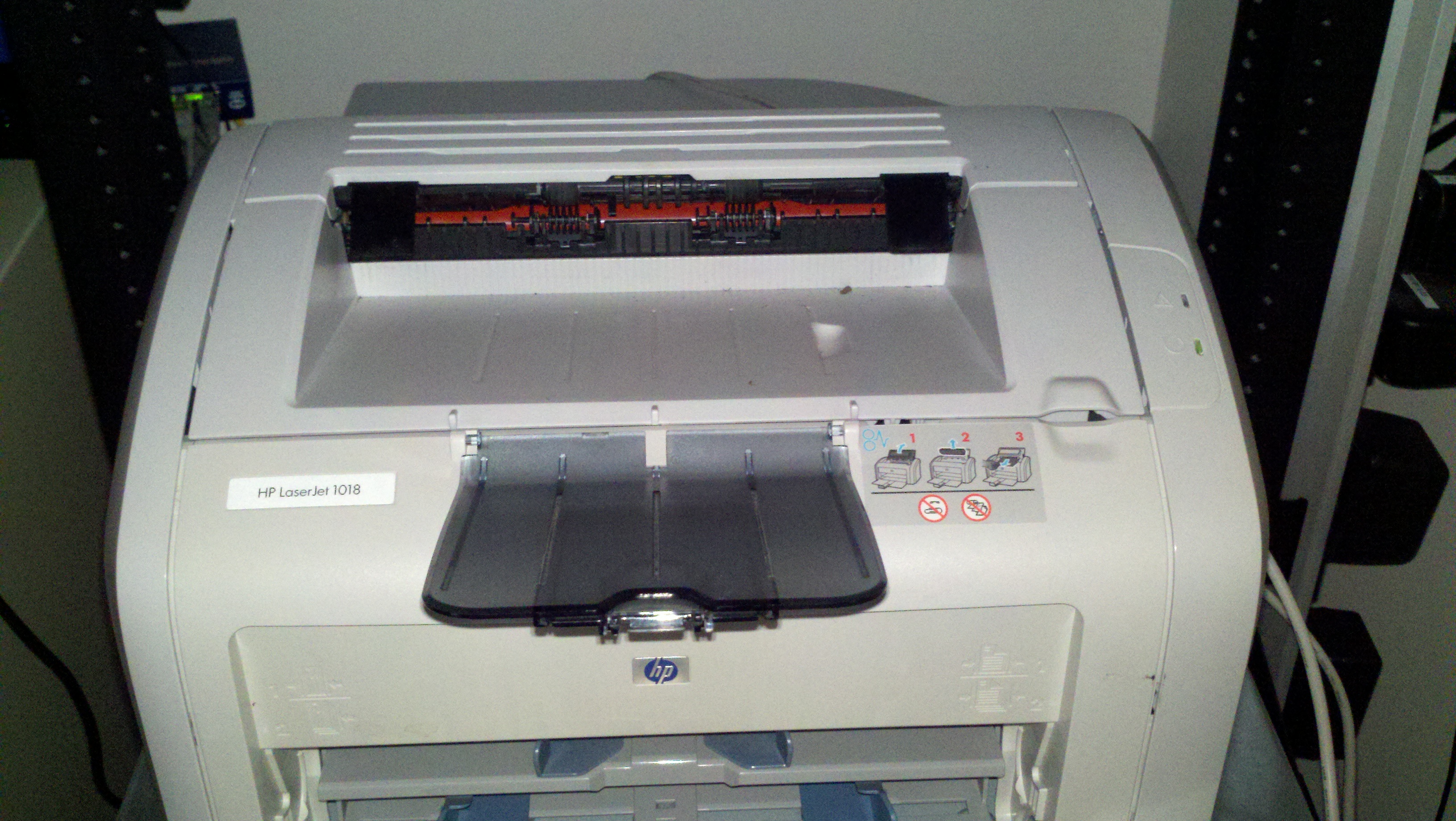
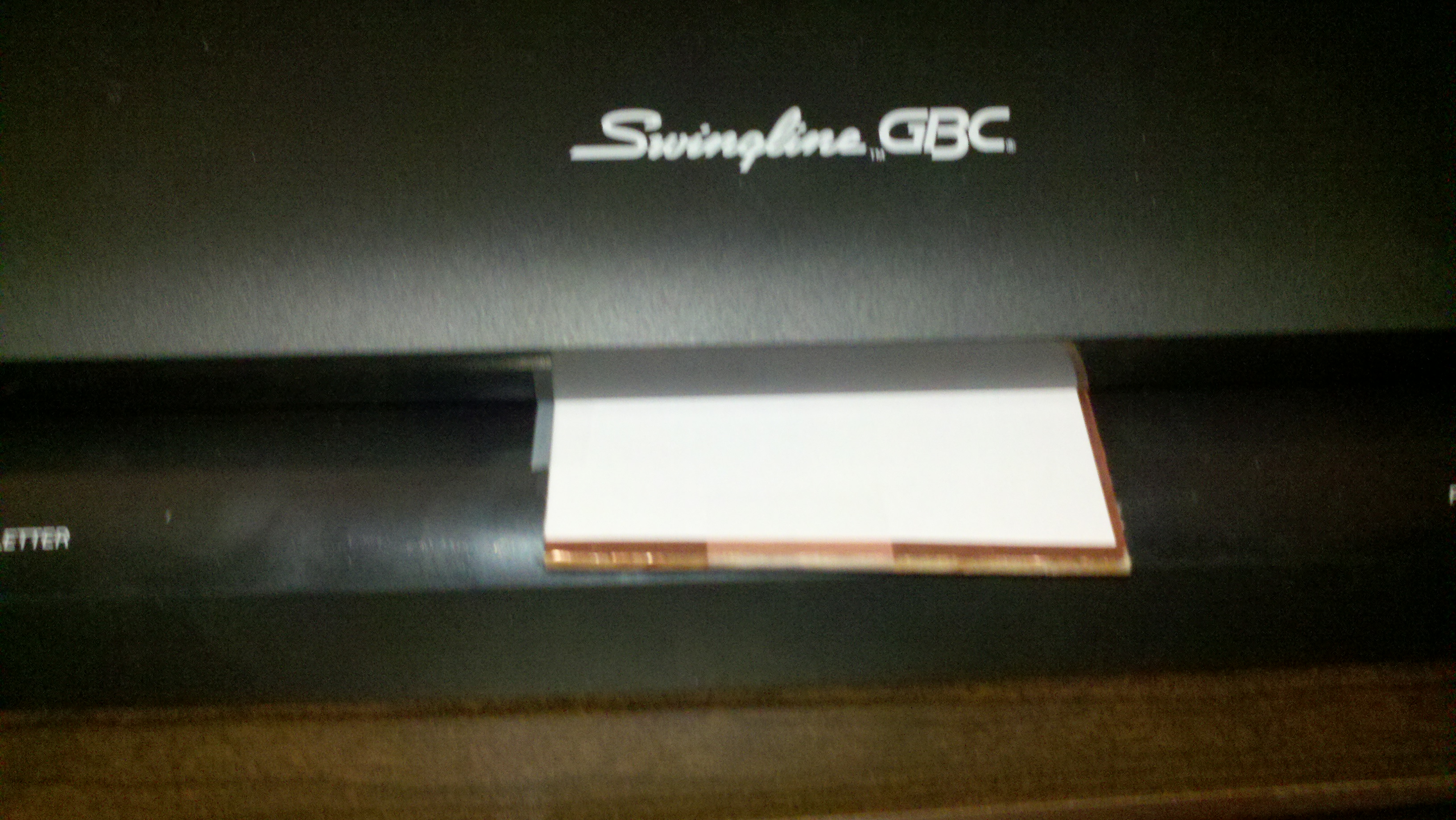
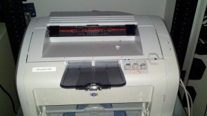
Second, a friend found a great deal on a HP Laserjet 1018 at a HAM fest for a whopping $5. No really, just five whole dollars that is it. Since we had problem printing on the paper we needed another printer and this one worked great. It printed fine on the toner transfer paper and it transferred cleanly and completely.
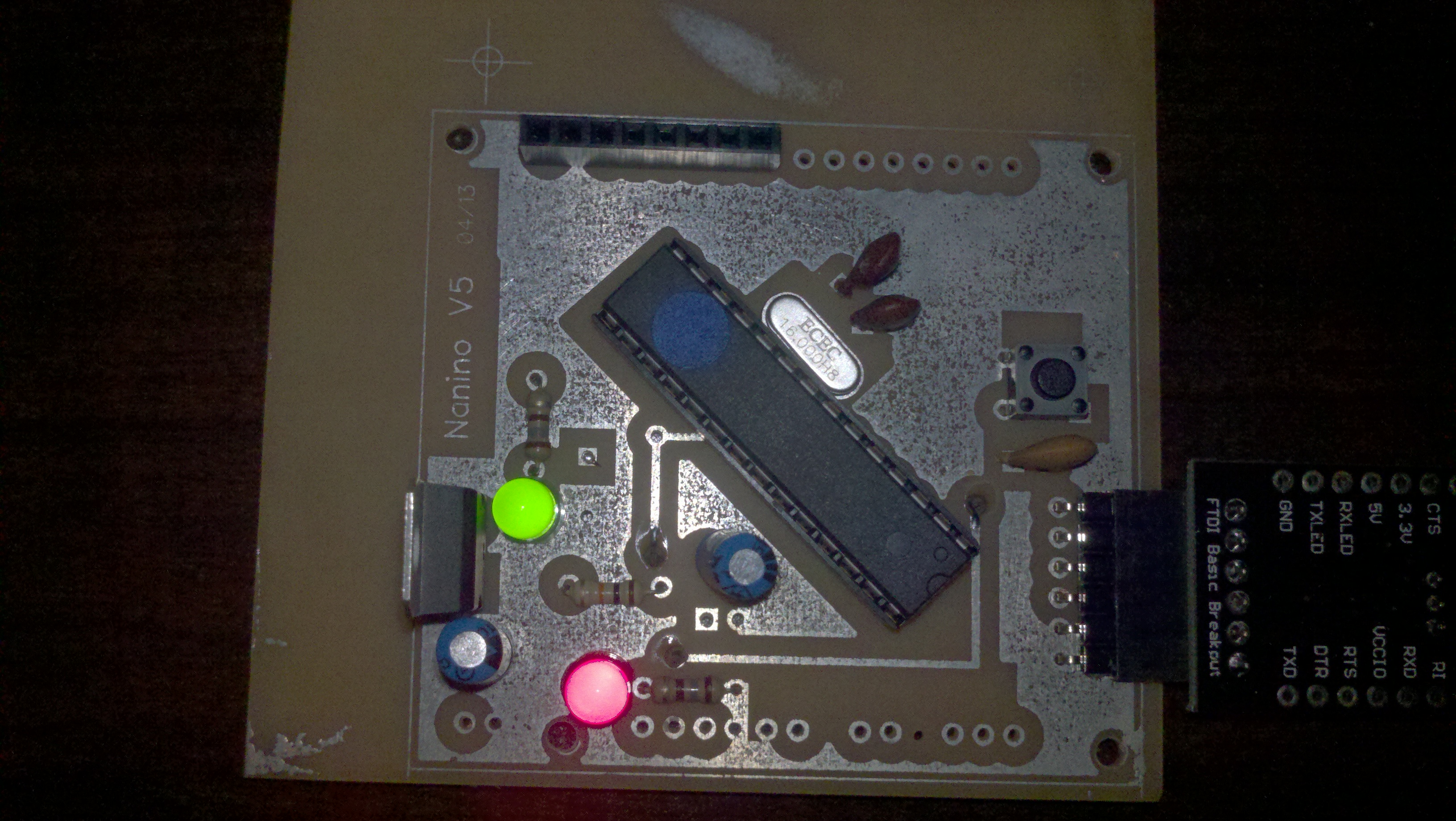
Third I modified slightly how I did the alignment of the top an bottom. Unfortunately I forgot to take pics to help explain the process (I will try to do better next time). Basically what I did was to take a scrap piece of PCB that is in an “L” shape. I took the top print (cut to approximate size) and taped it to the “L” scrap. I next used the registration marks and center punched and drilled a hole through the board. Next I used the holes to align the bottom print using the registration marks and shining a light through the paper. I then slipped the PCB I was going to tech into the “pocket” and taped the prints to the board. Finally I removed the scrap. I realize that this is a bit difficult to explain an I promise that next time I will snaps some pics. Ultimately the alignment is spot on and I am very happy with the results as you will see in the pics below.
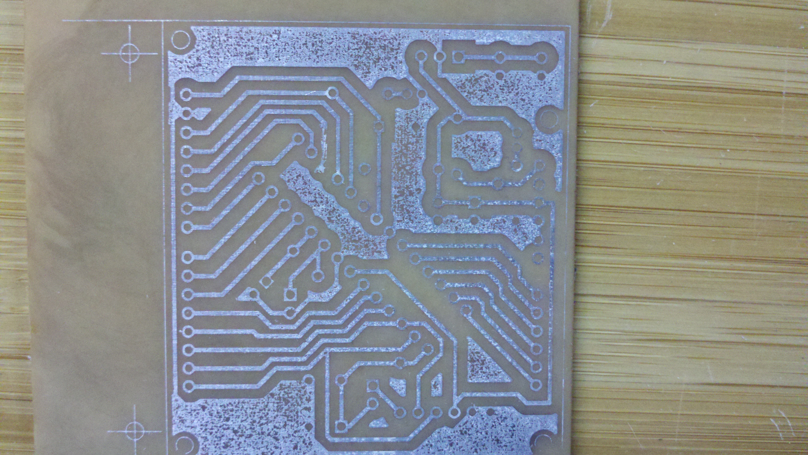
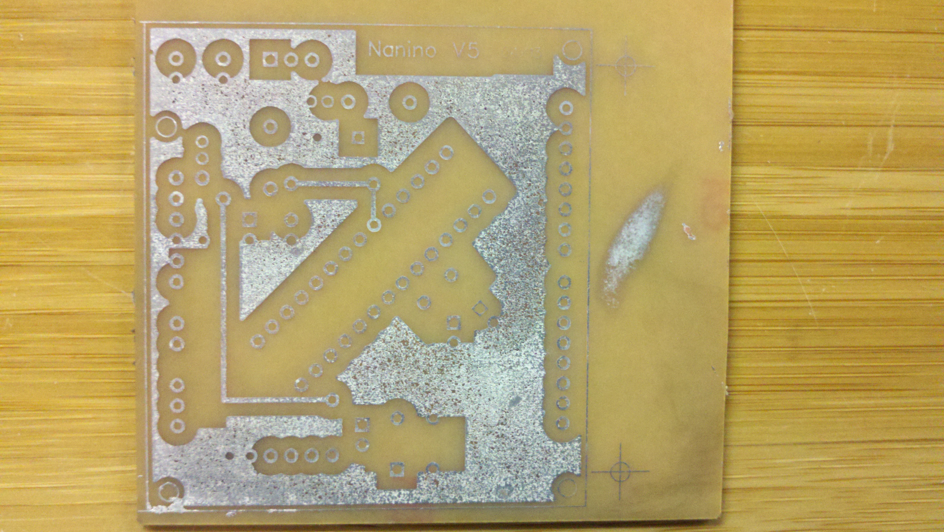
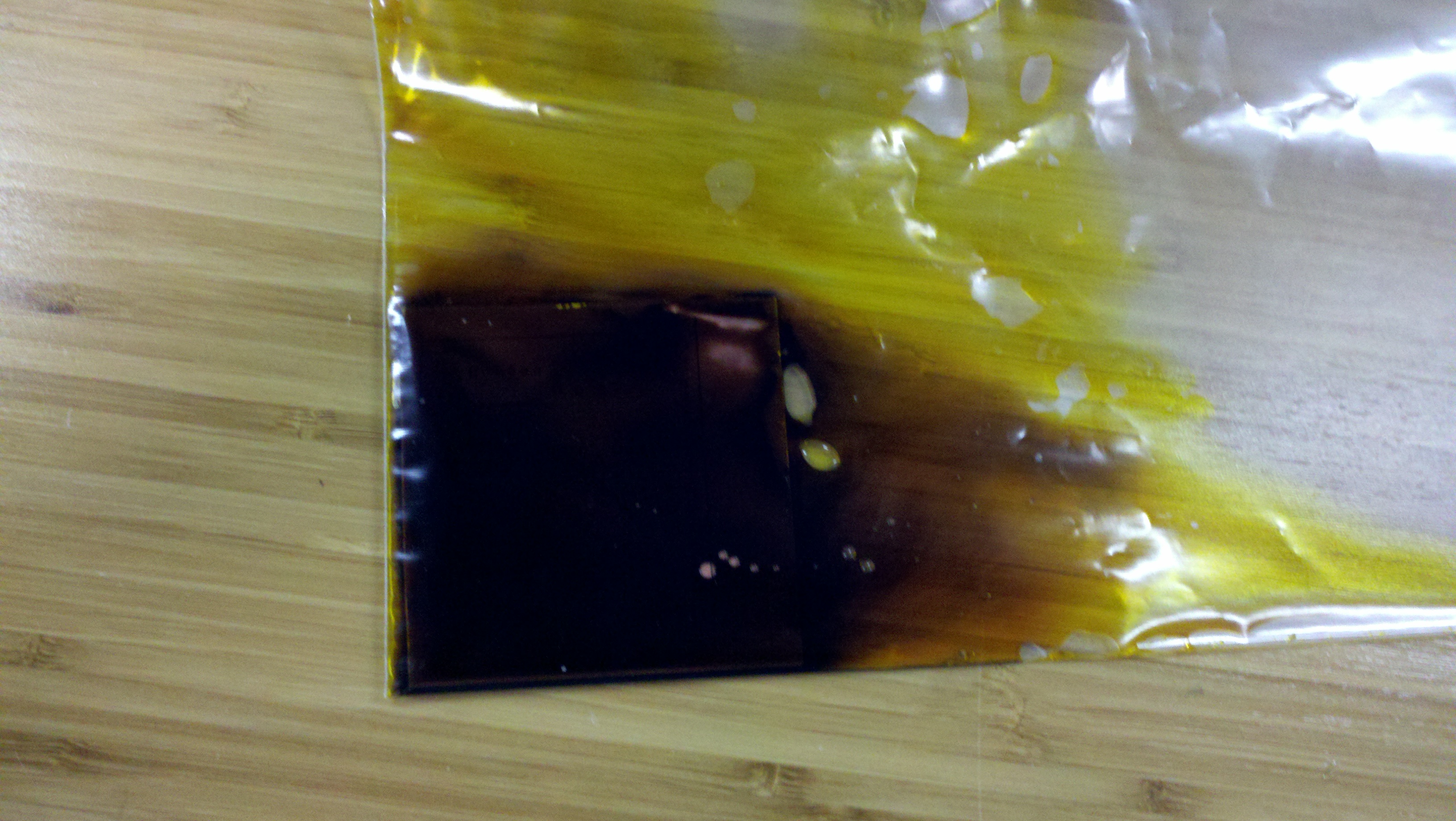
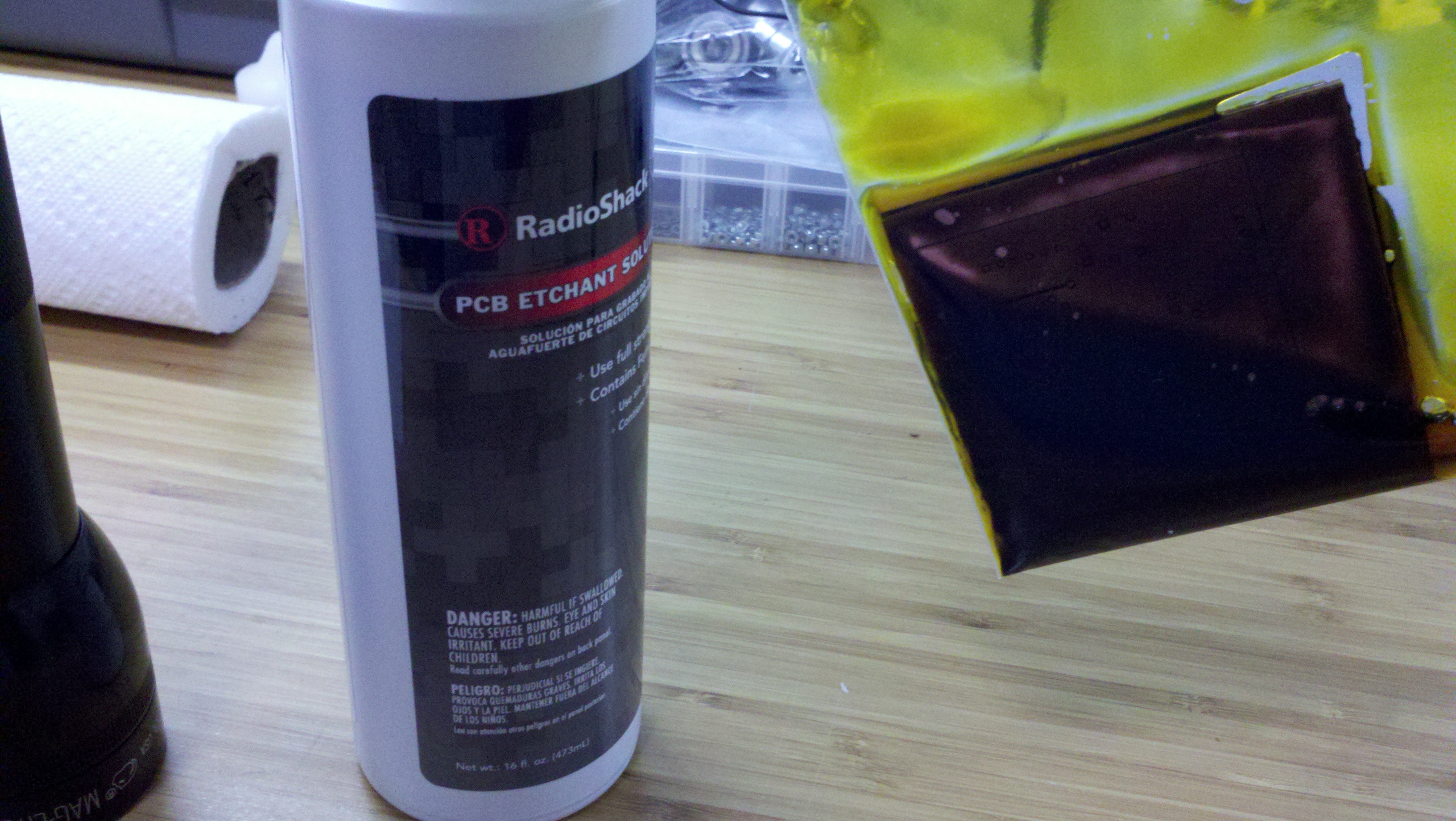
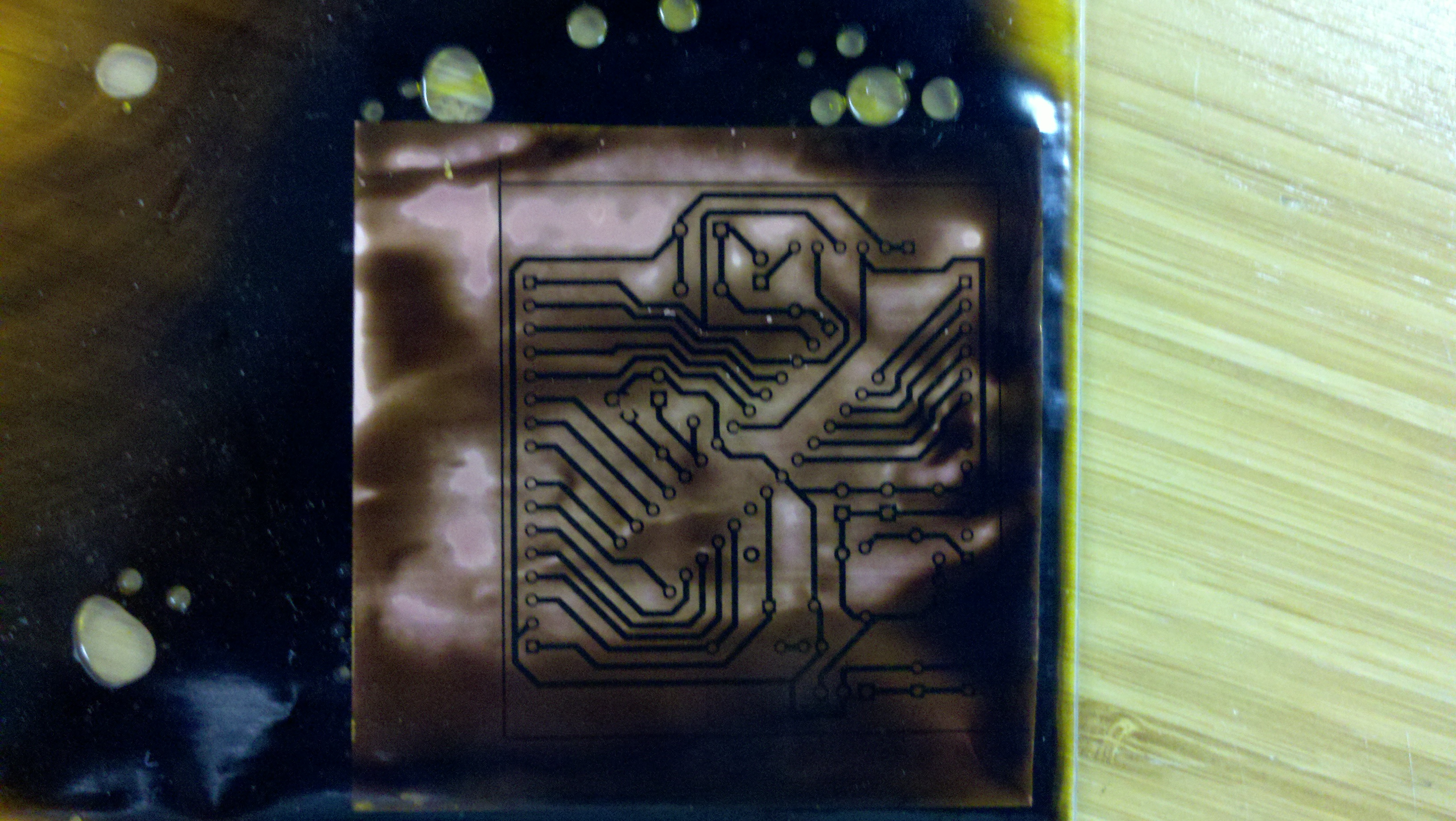
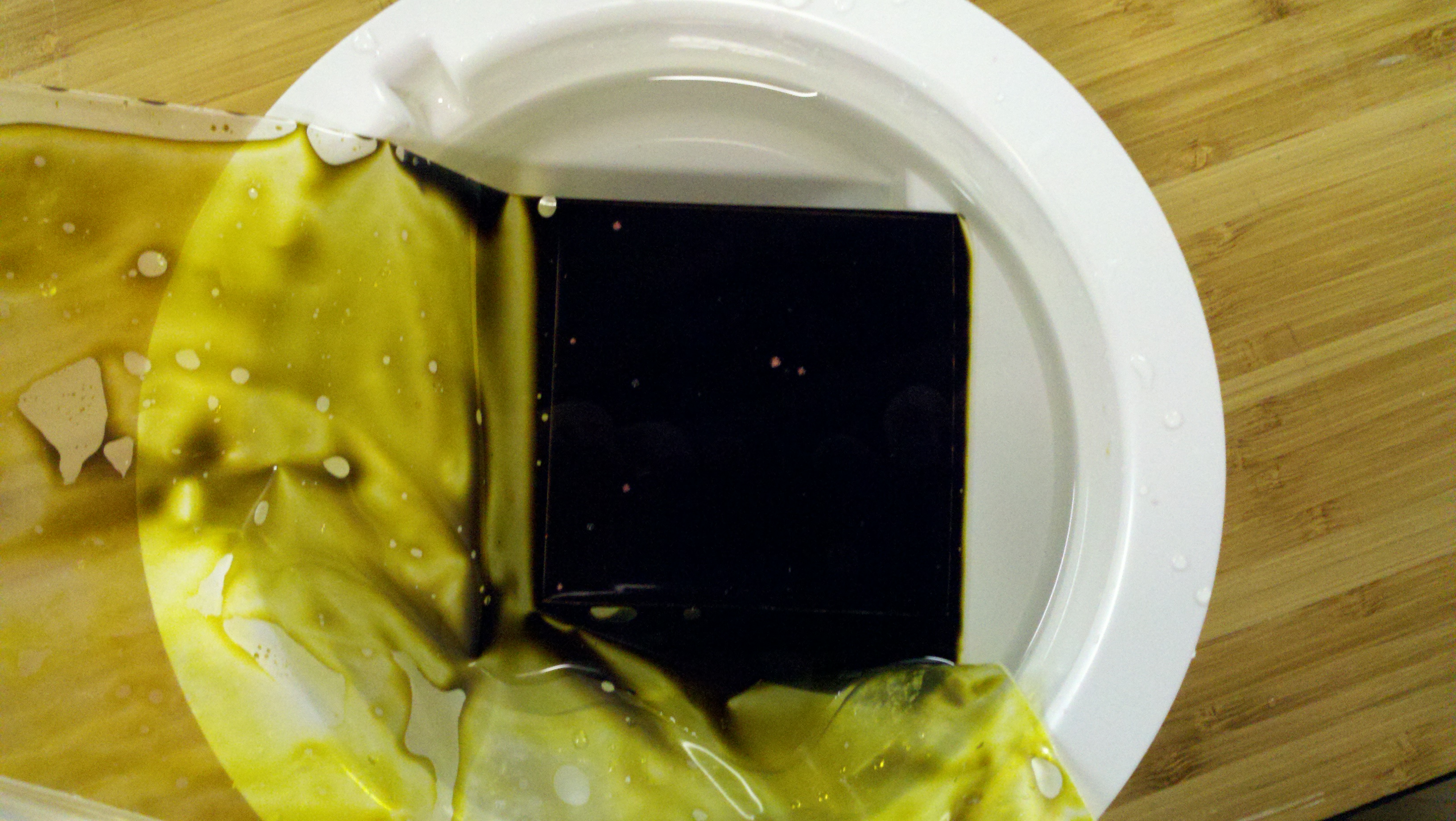
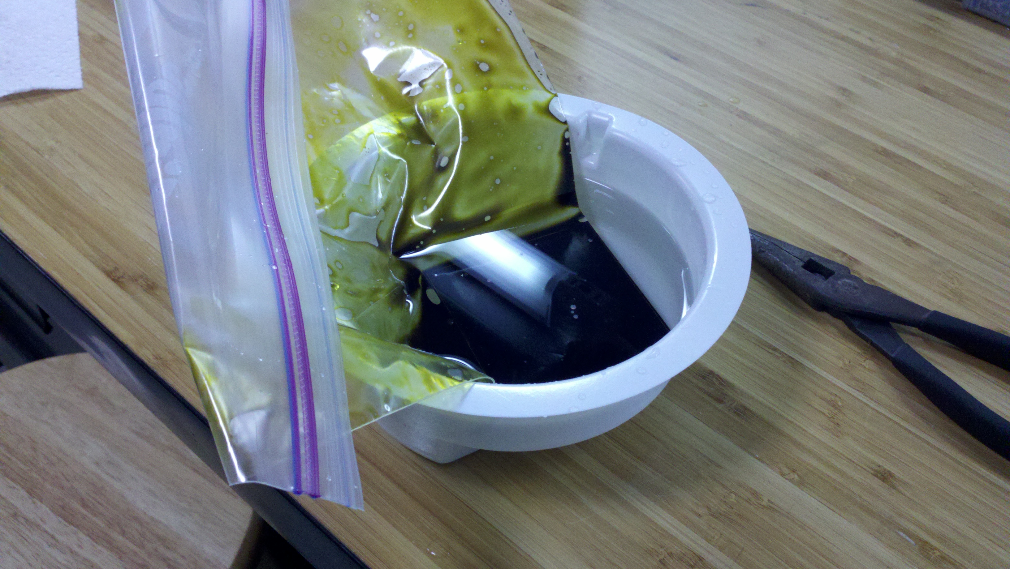
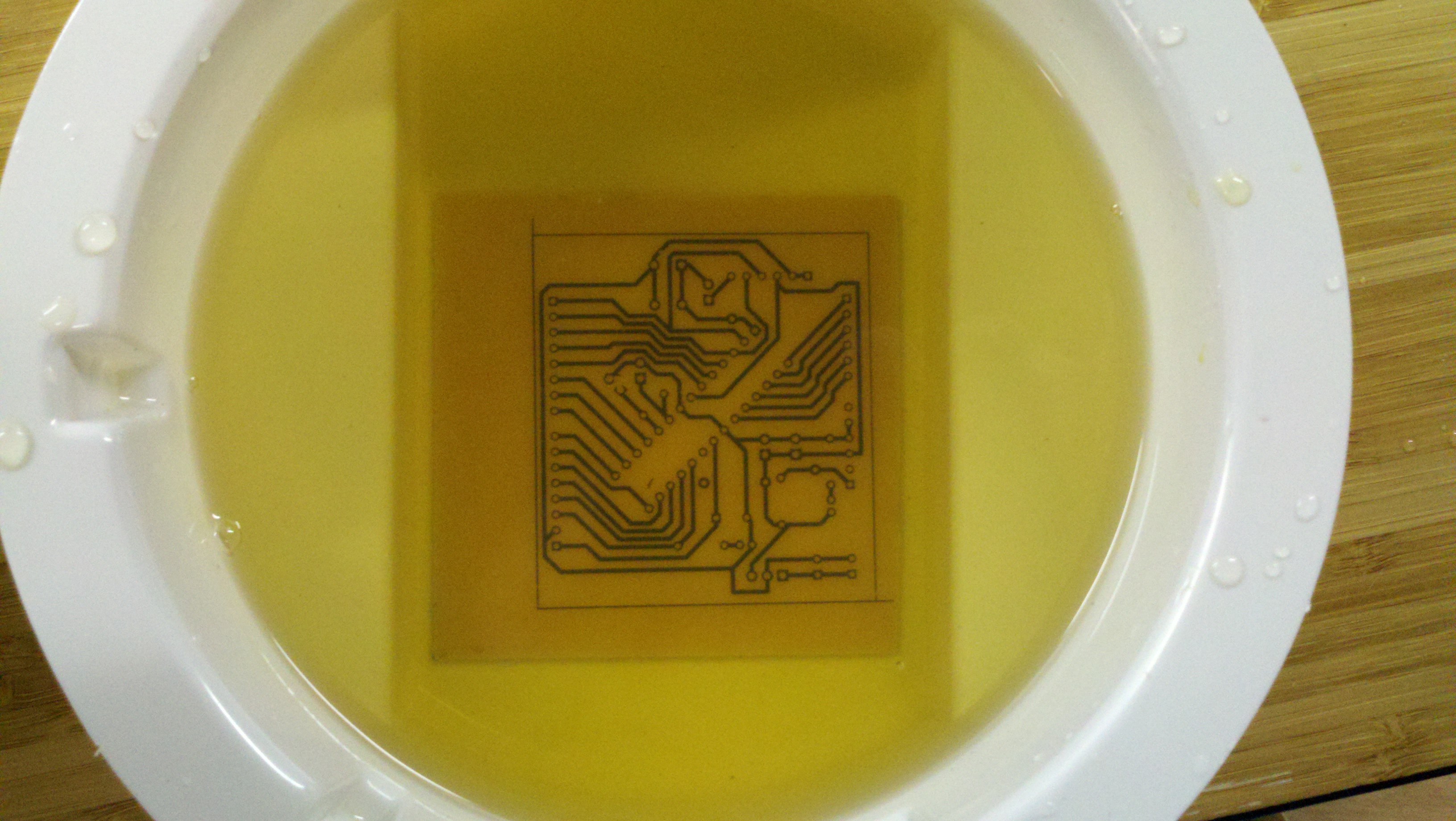
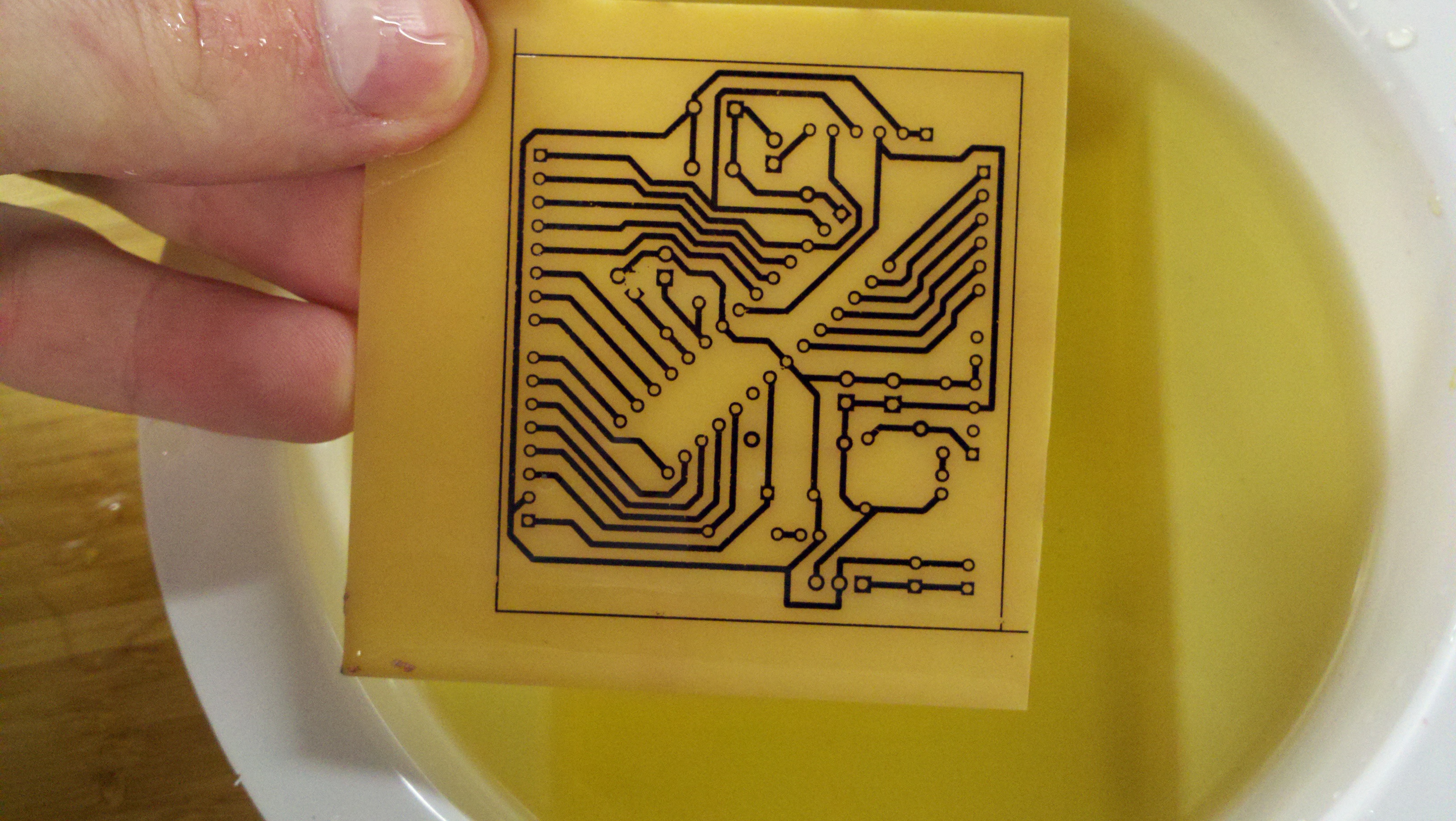
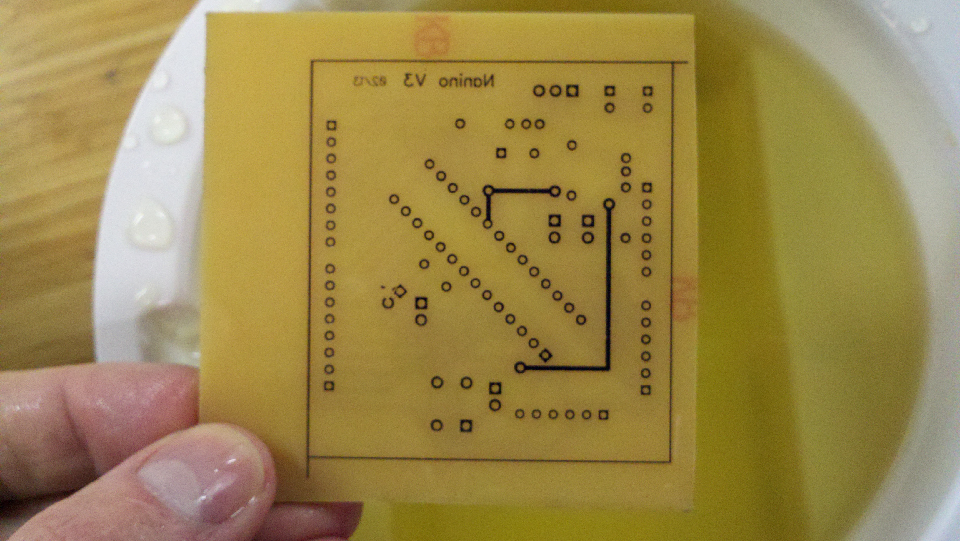
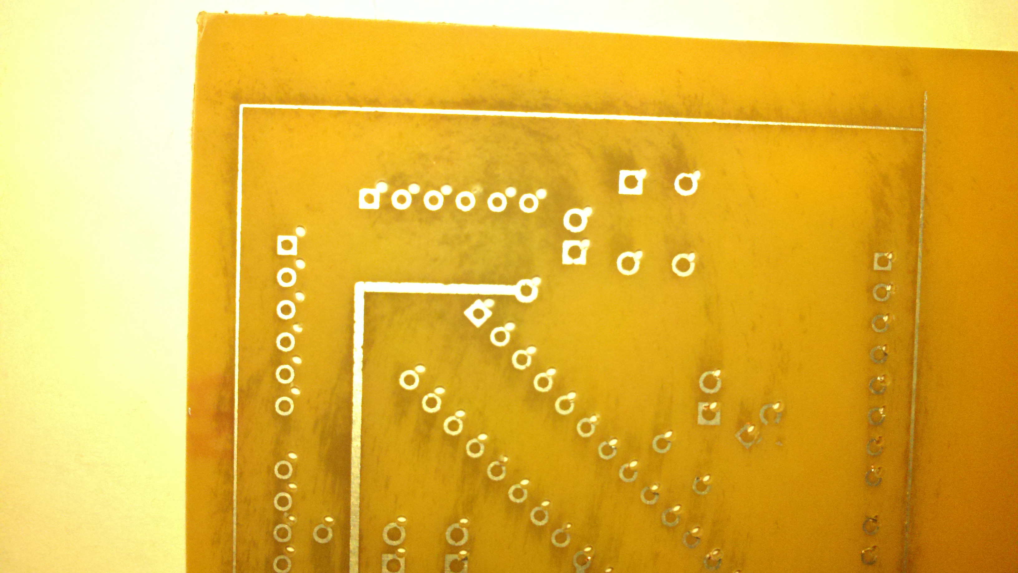
So far so good, now what? Well apparently I didn’t read my lessons learned from my previous attempts and I forgot to rinse the board after doing the transfer. This made it take forever for the board to etch. Even longer that before. I ended up leaving the board in the solution for 45-50 mins. This cause other problems it seems that the acid got through the toner an started to pit the copper pores. It does not appear to have adversely effected the functionality of the board but, it does not look a nice as it should. Also during the etching phase I learned another lesson. I was placing the PCB in a zip lock with the ferric chloride and this tended to leave bubbles and places where there was little to no solution. I do not think that I will use this technique again and instead just place it in a tub.
So without further adieu
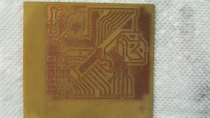
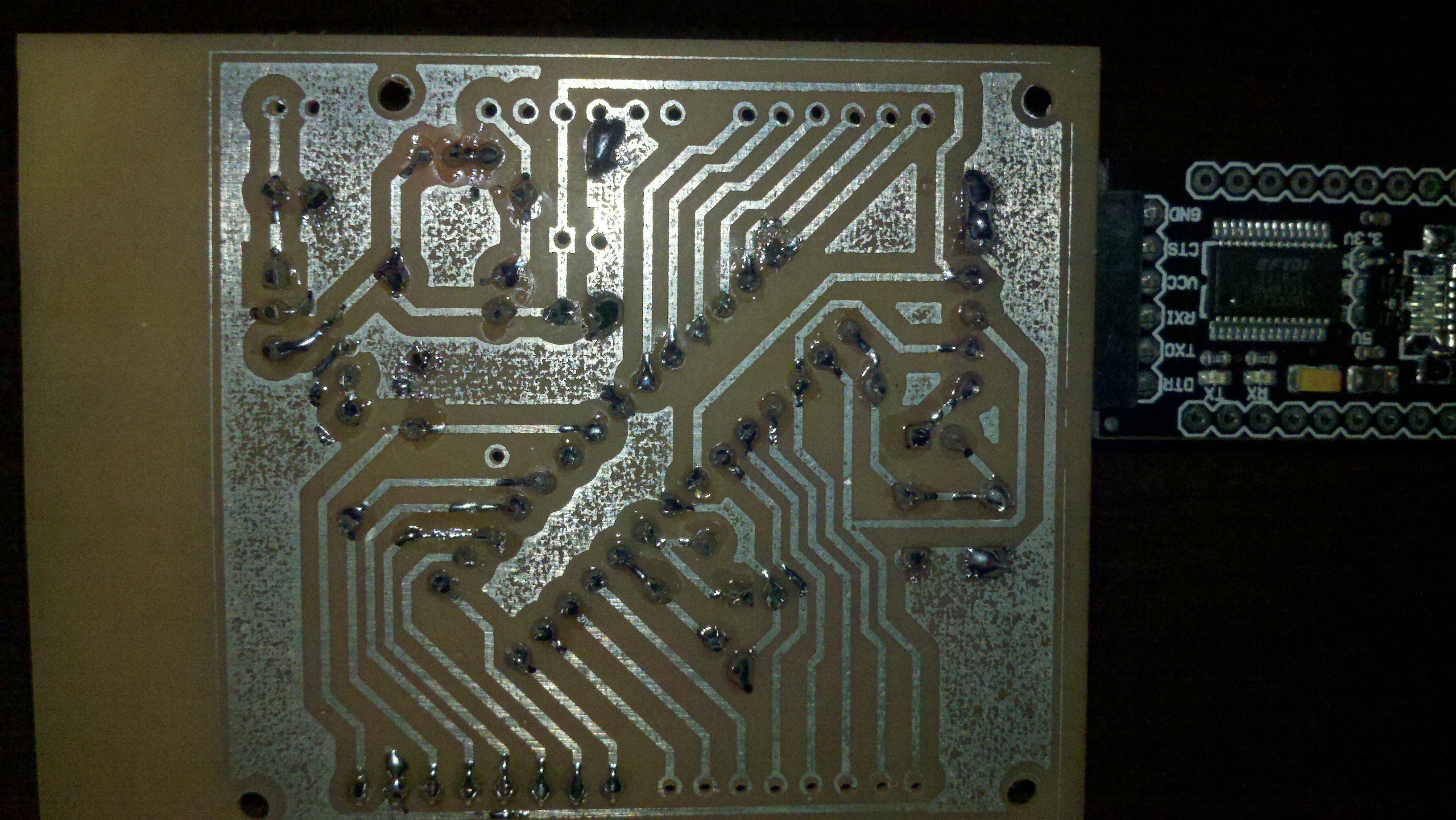
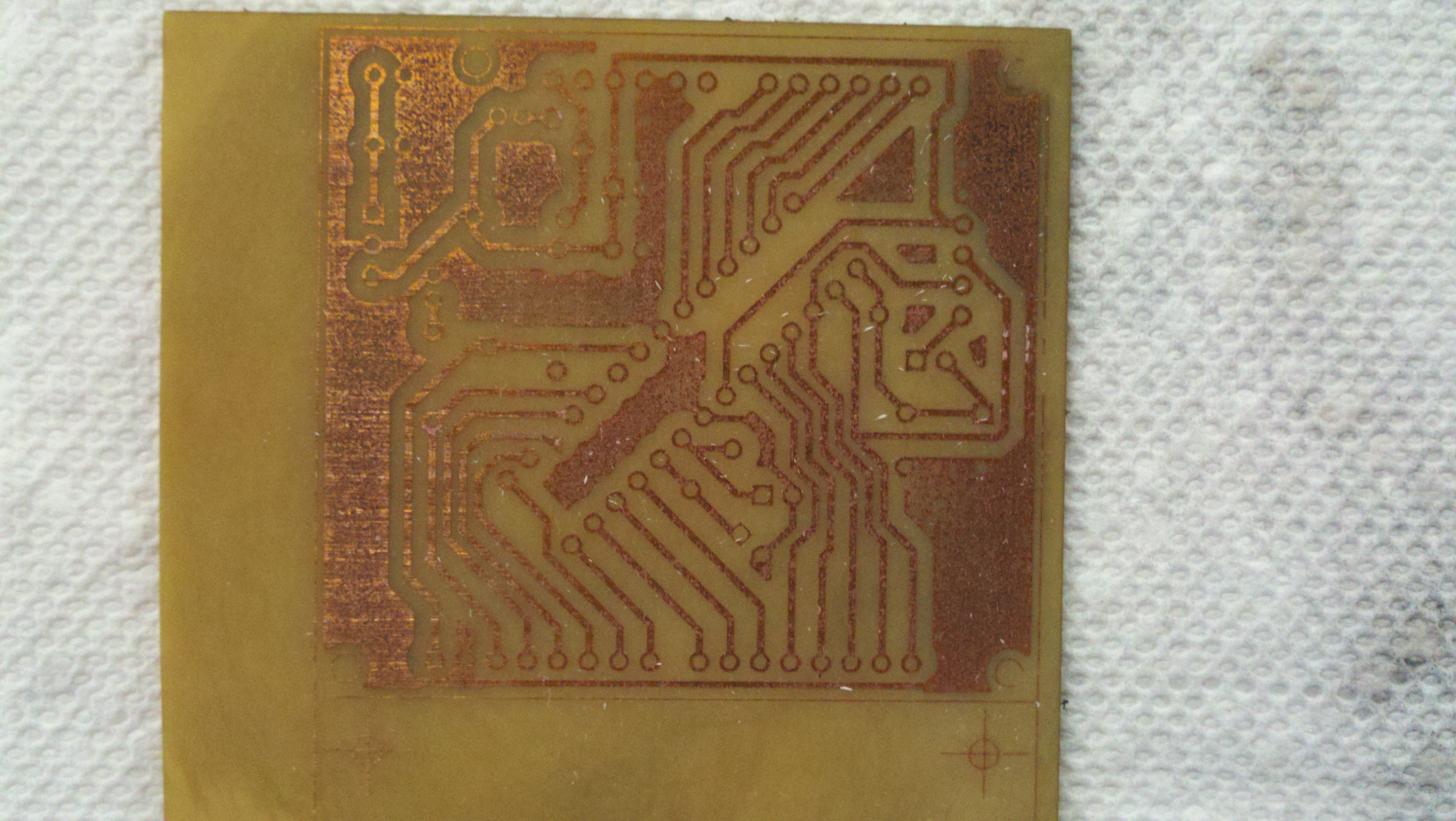
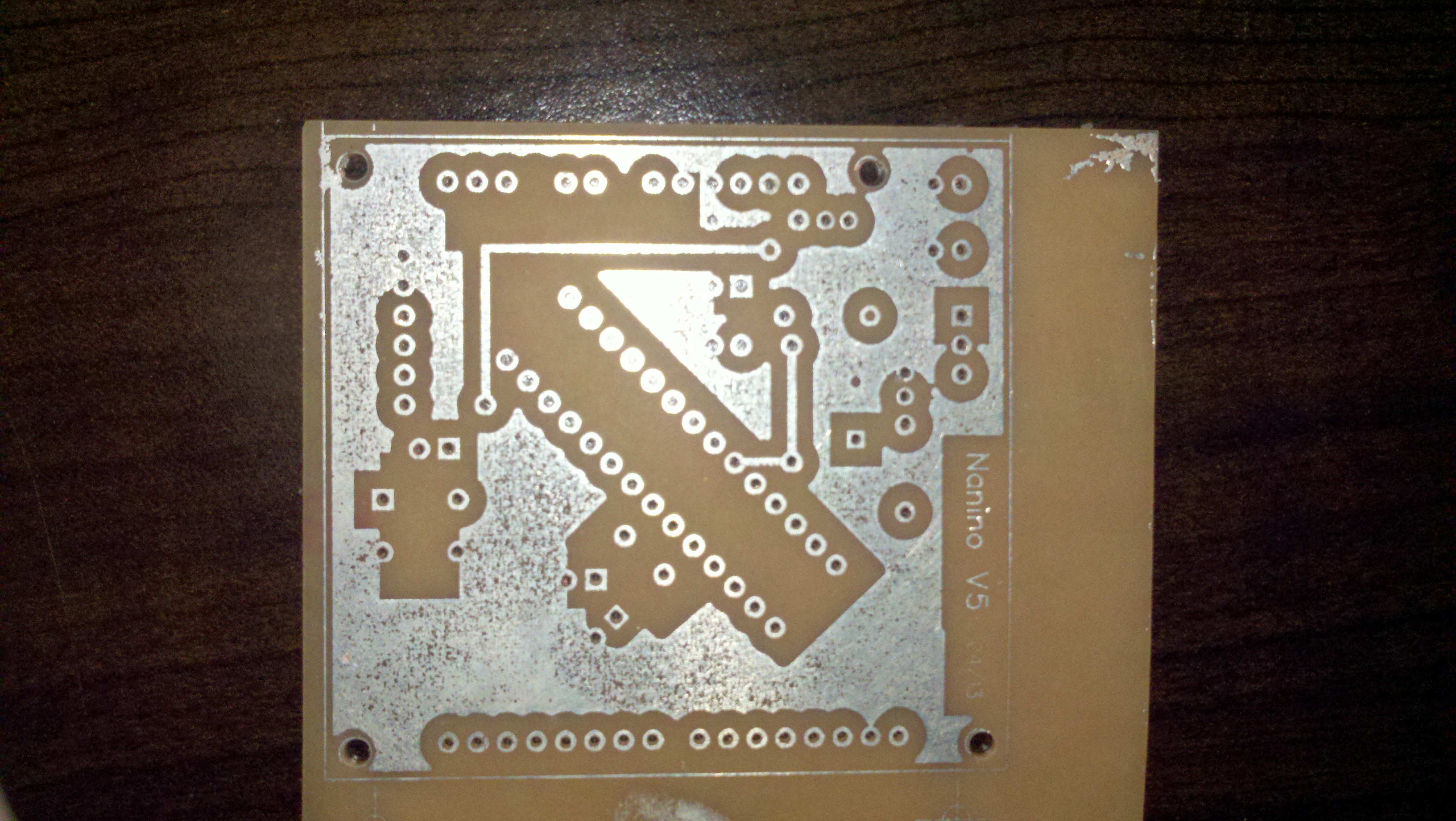
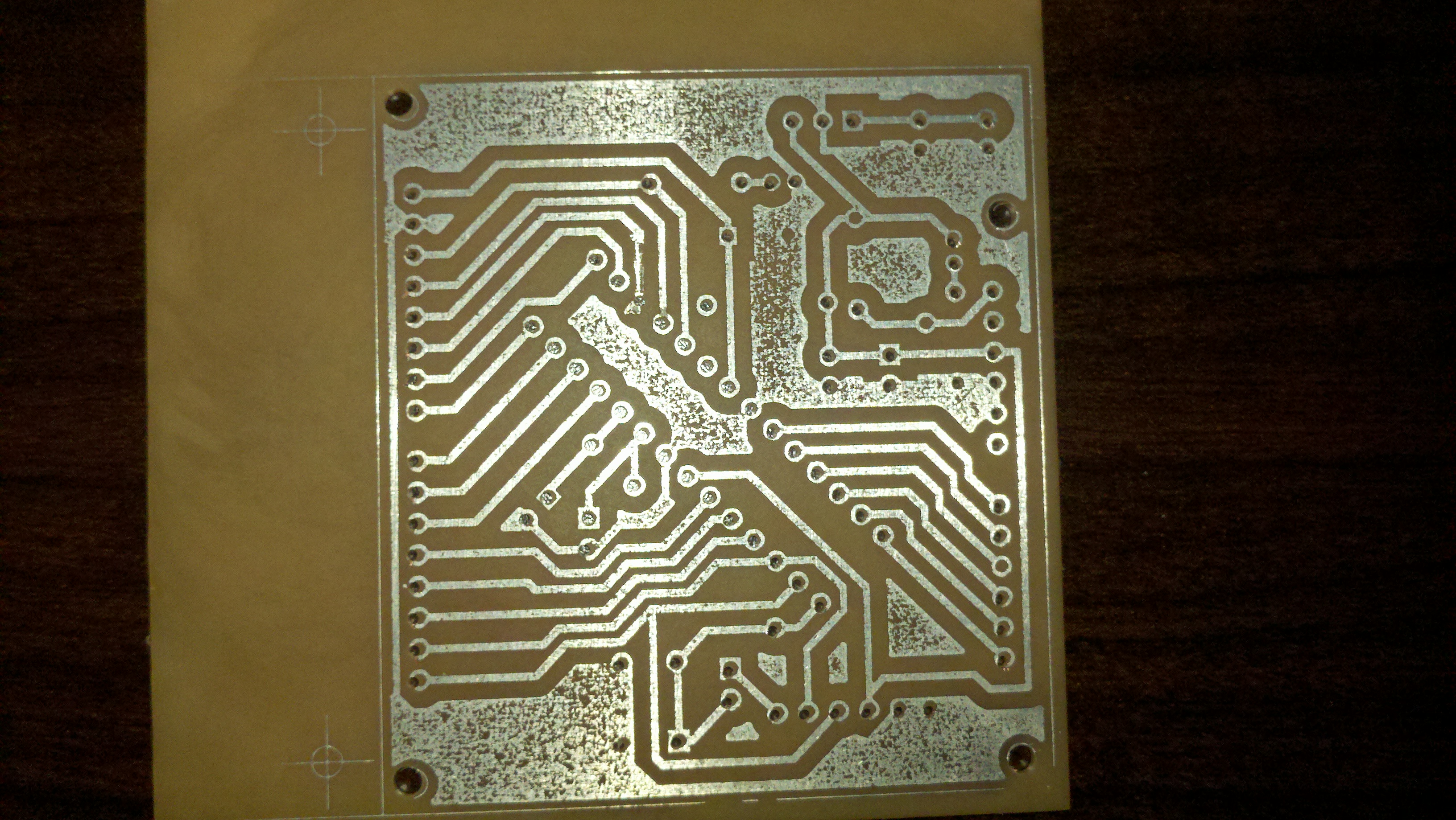
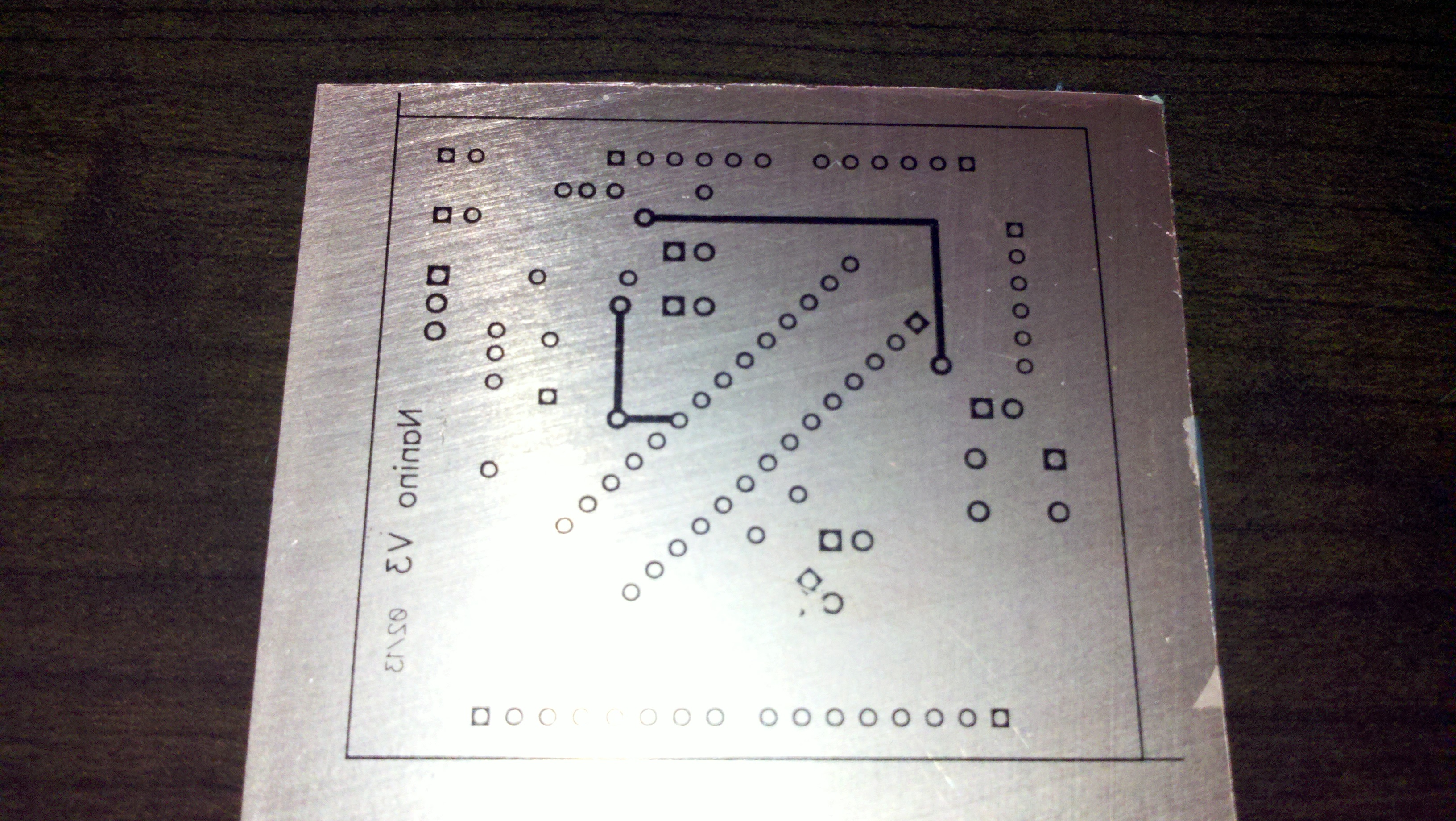
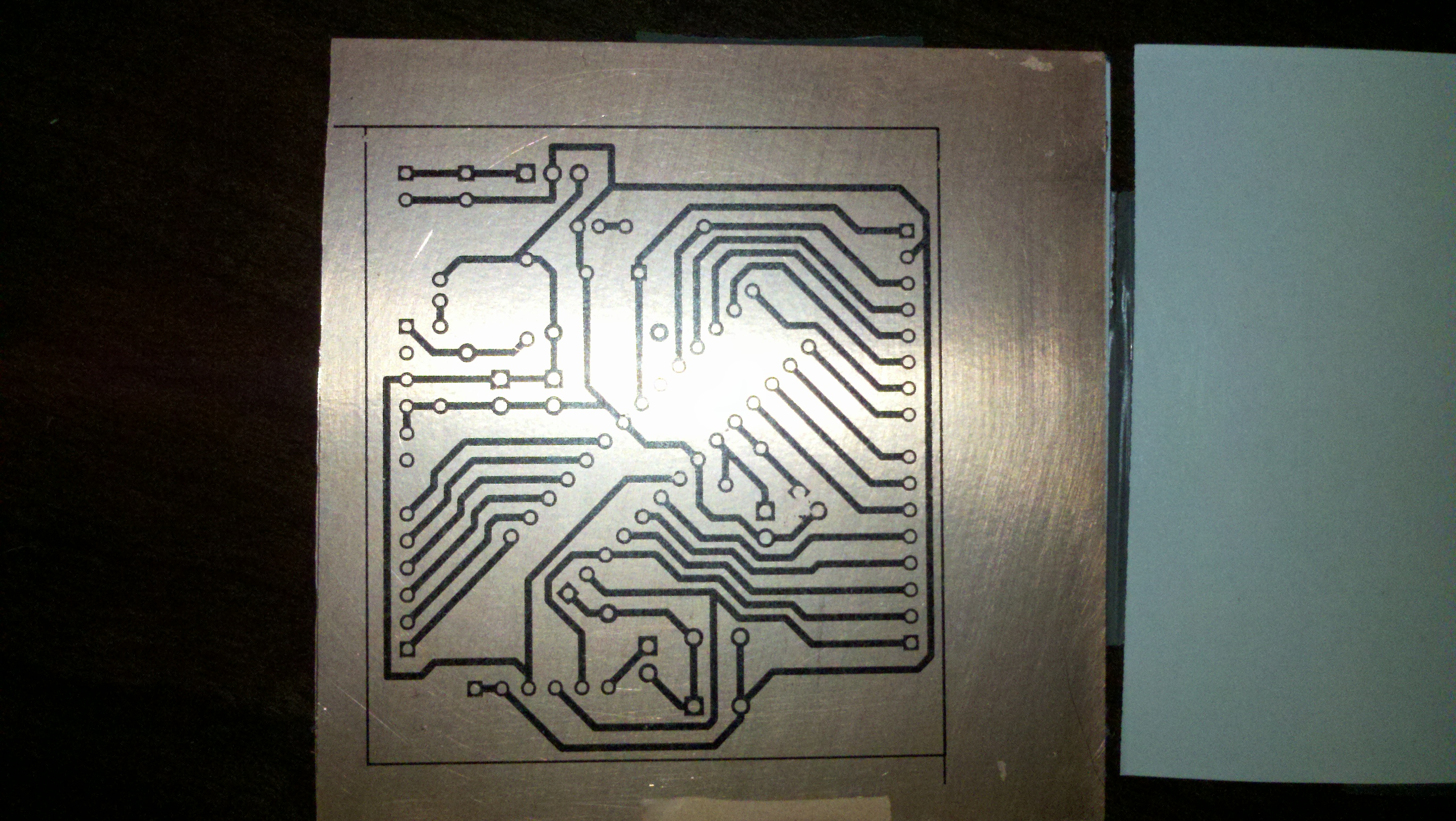
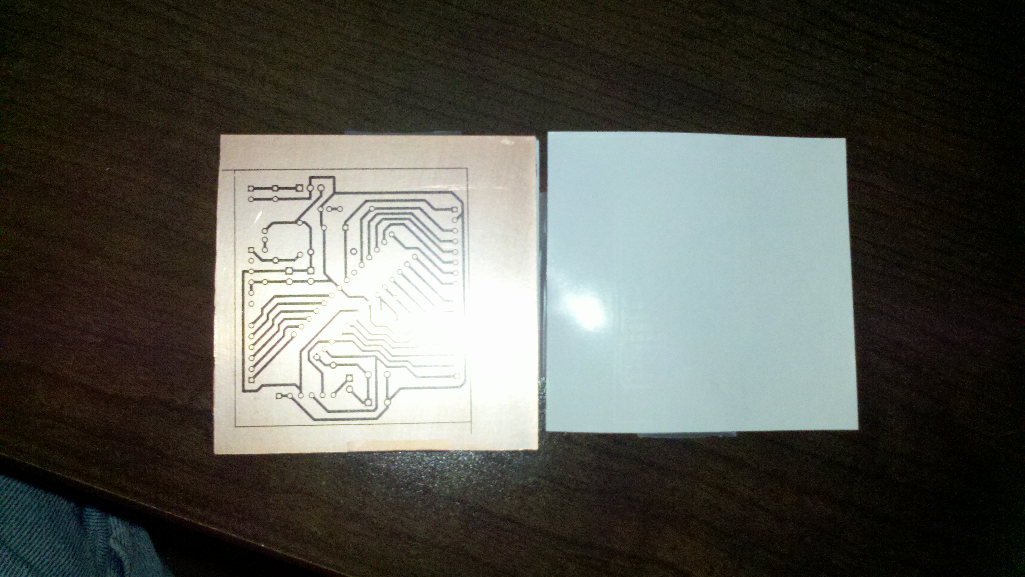
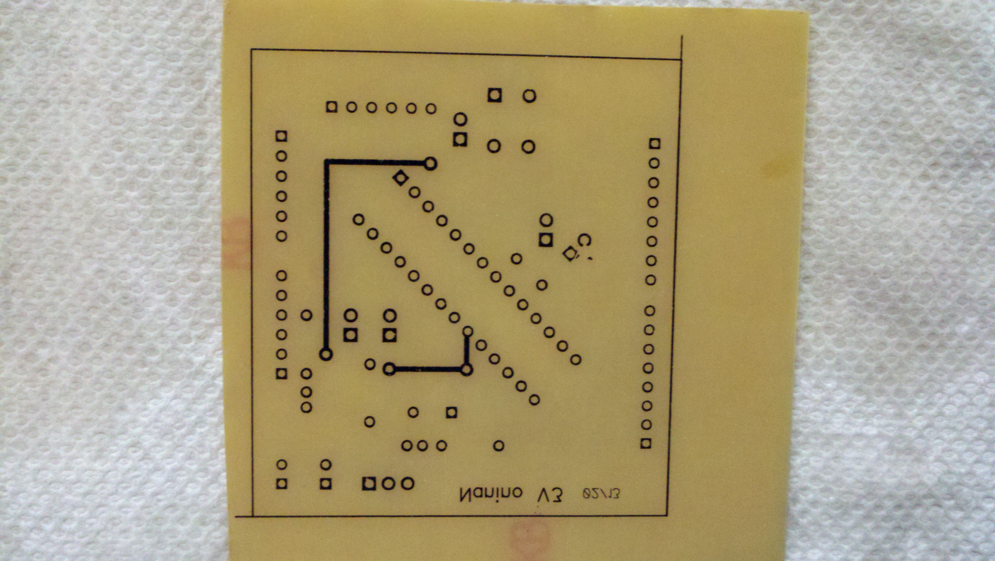
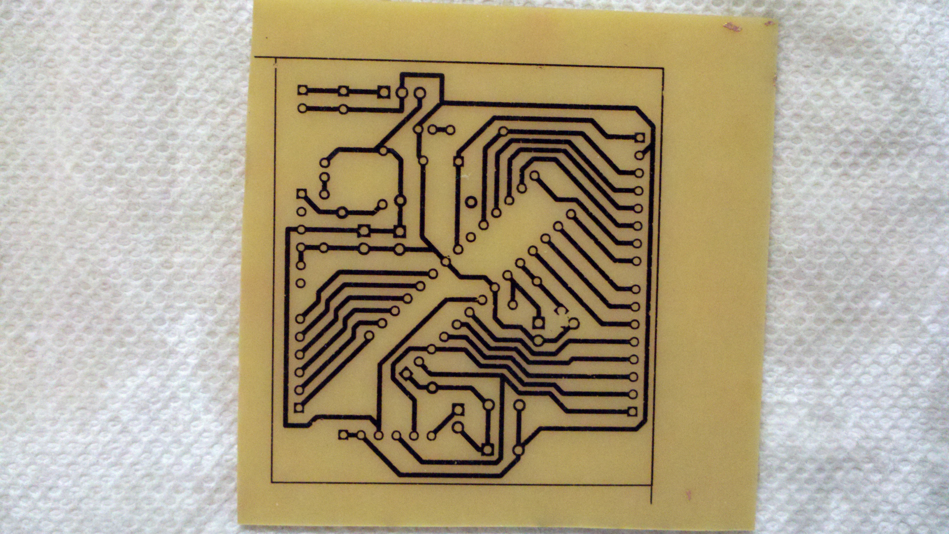
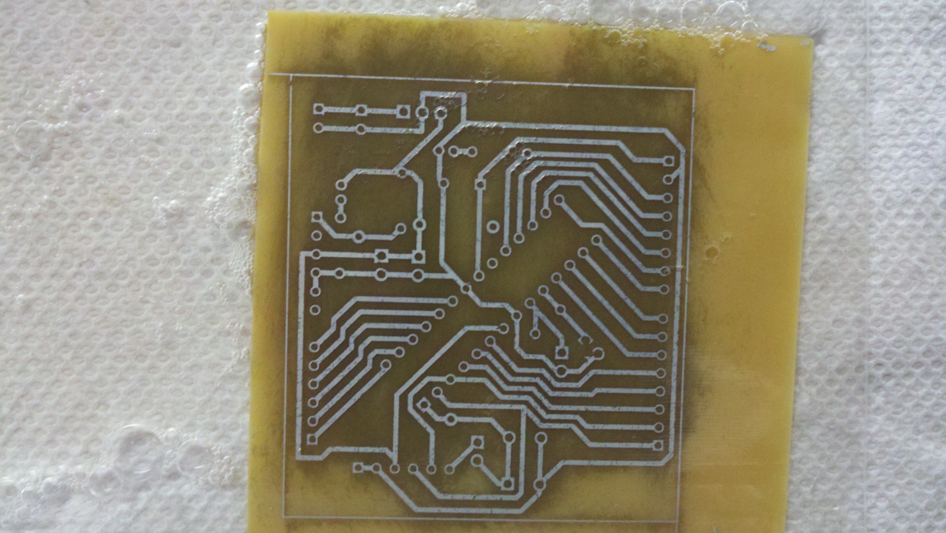
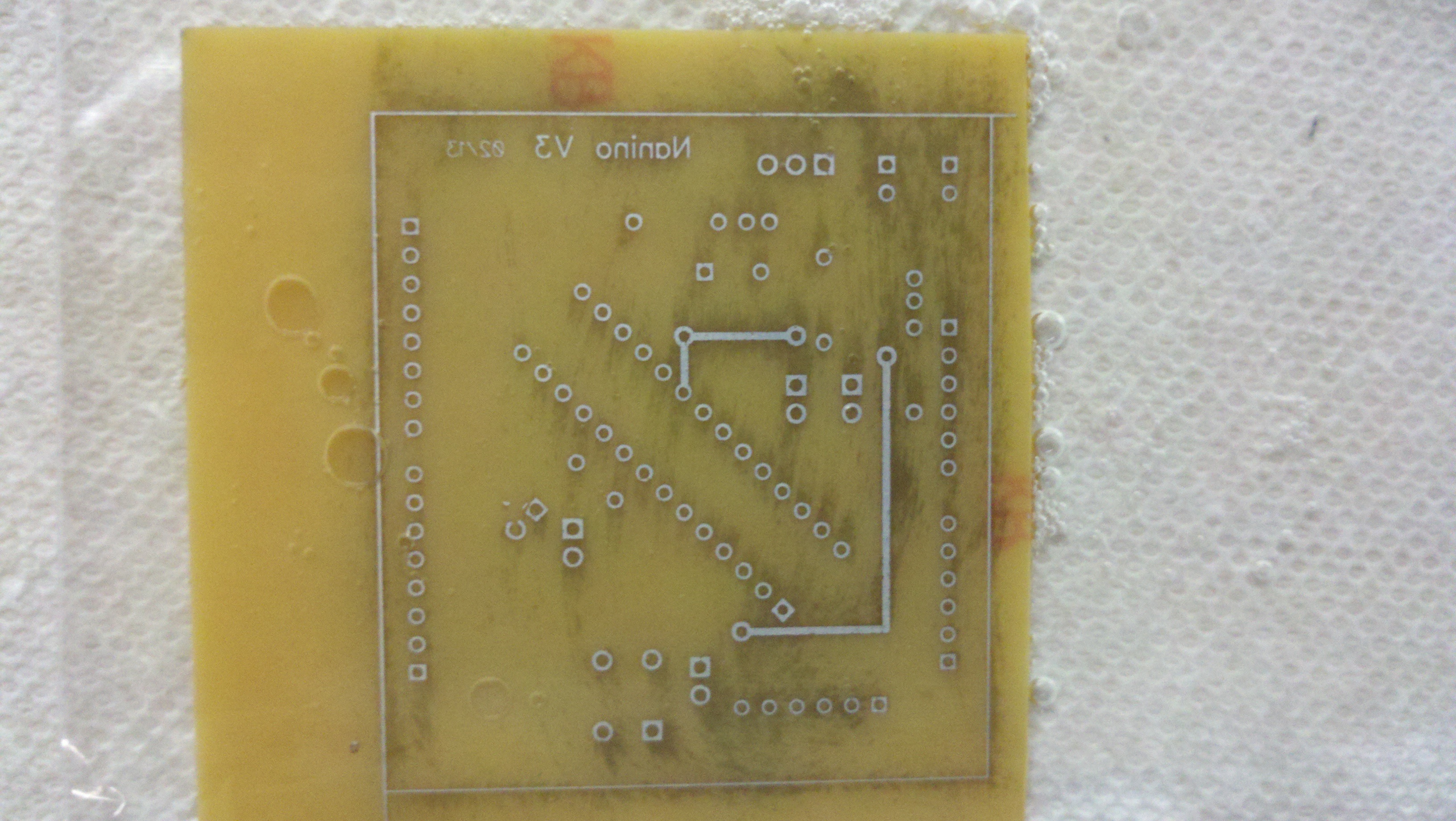
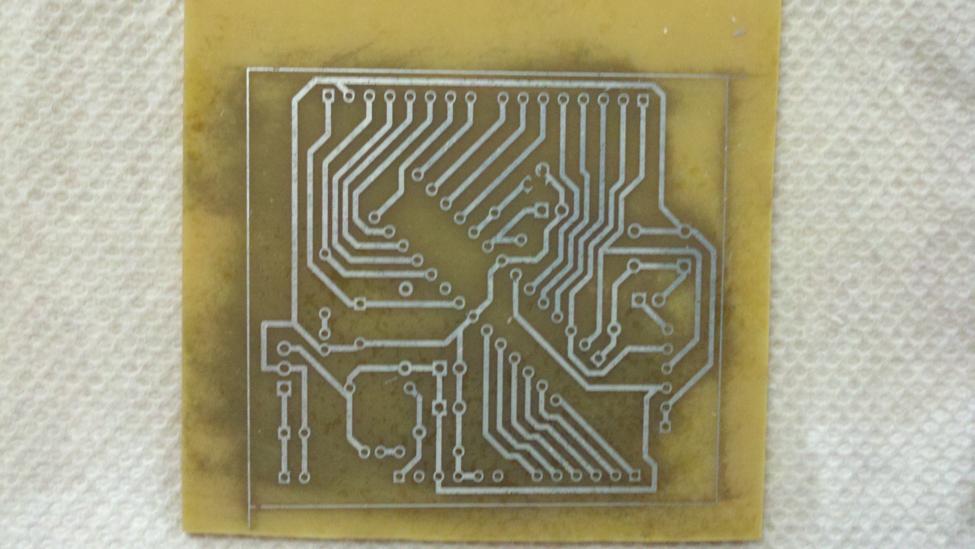
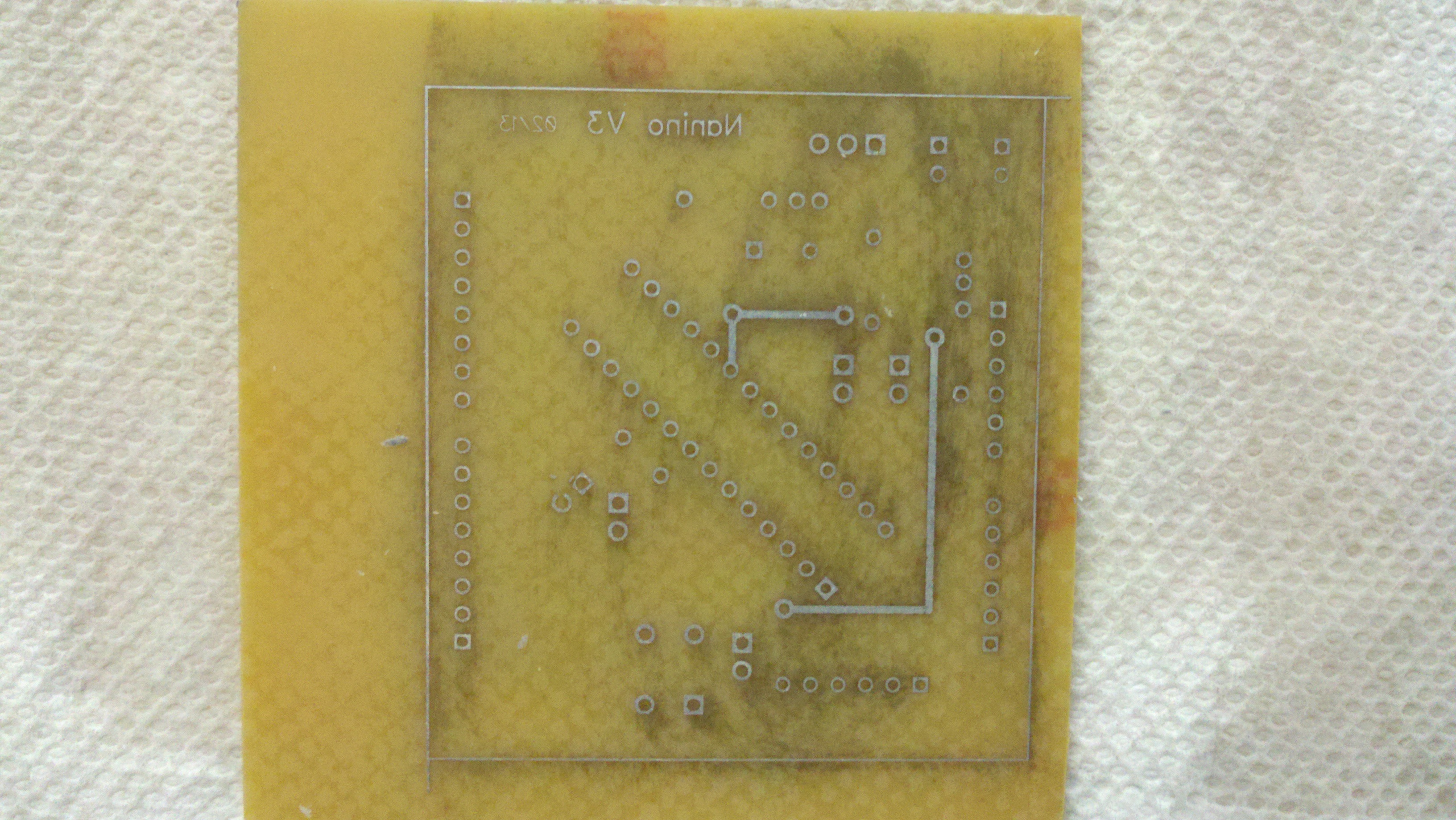
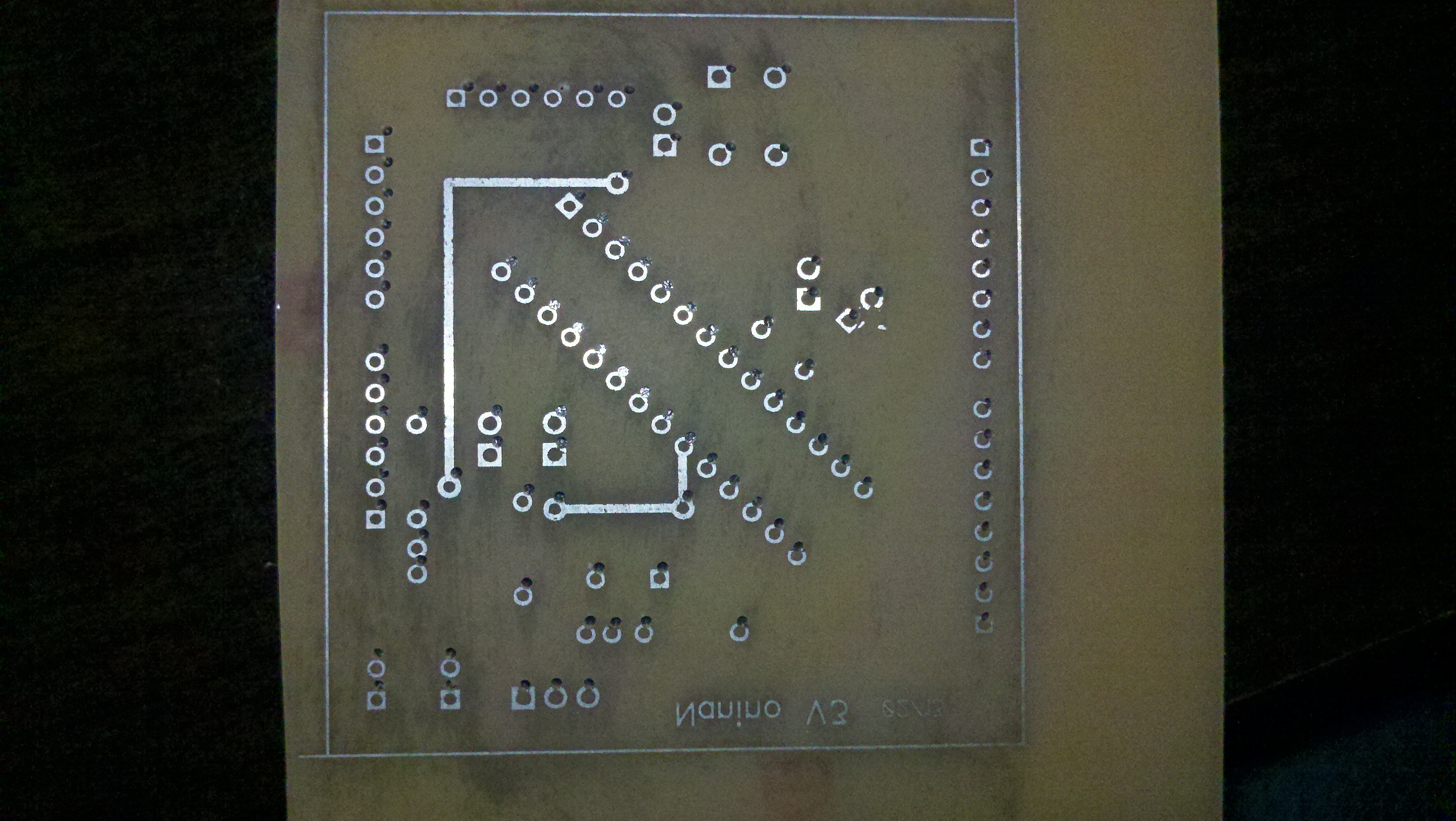
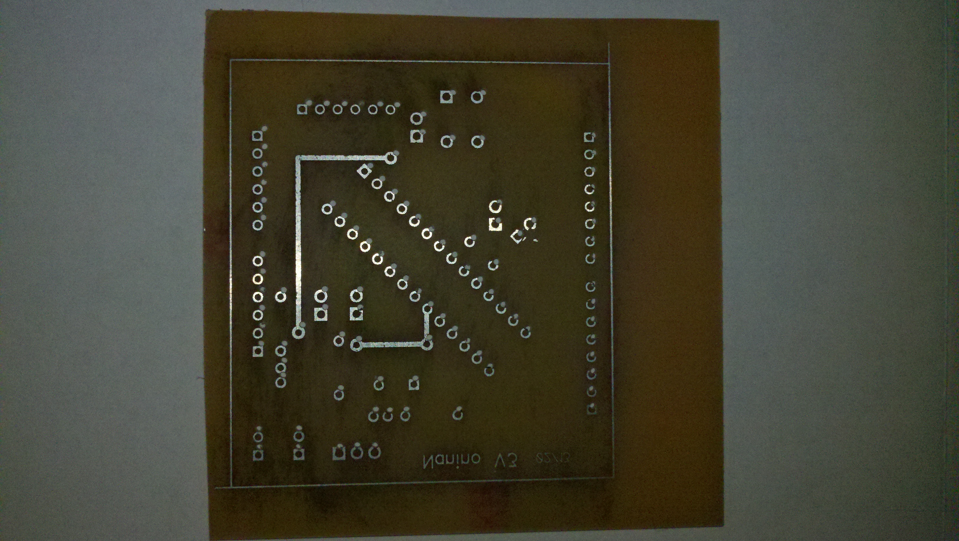
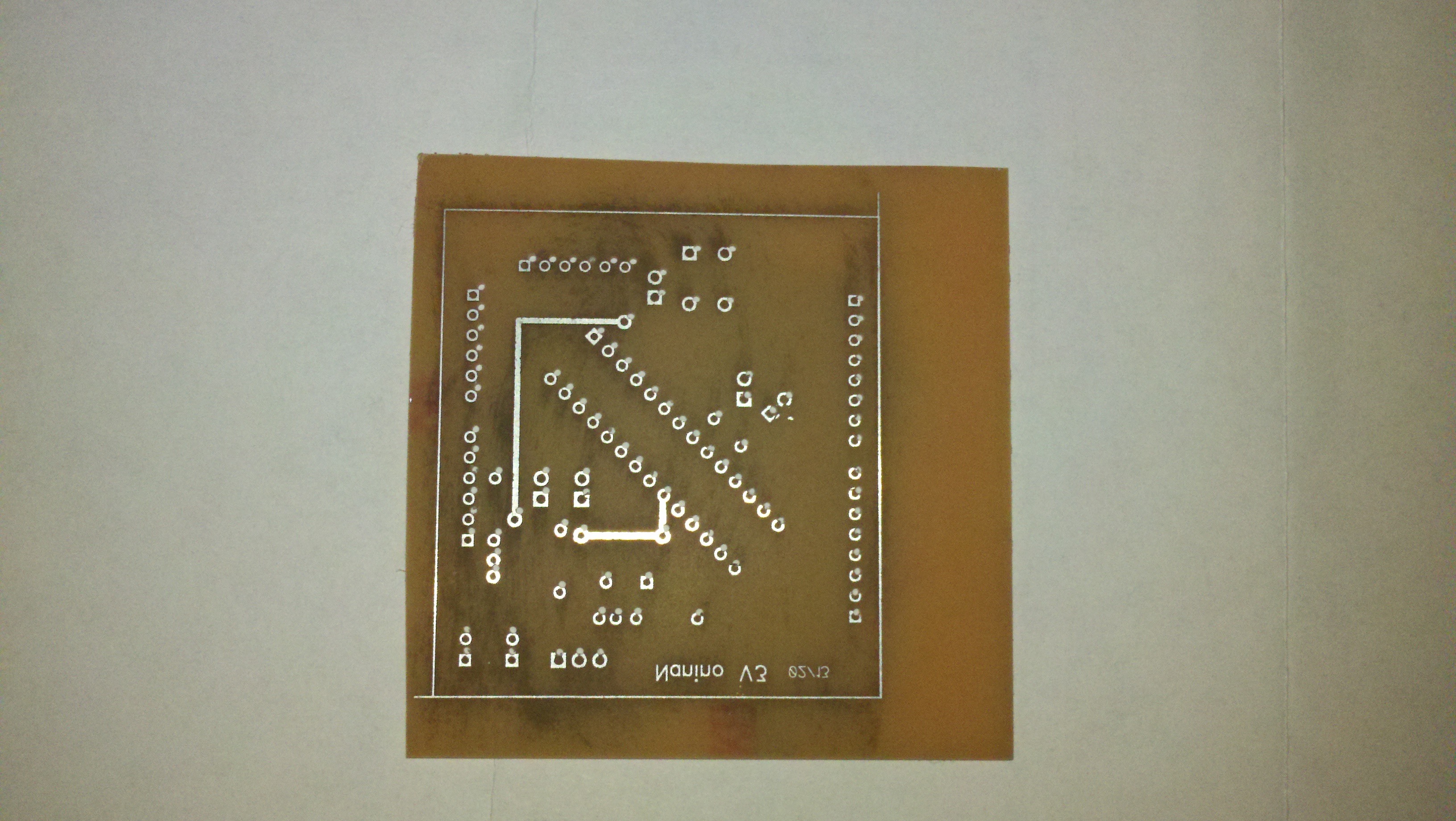
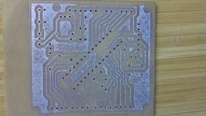
Etched bottom toner removed
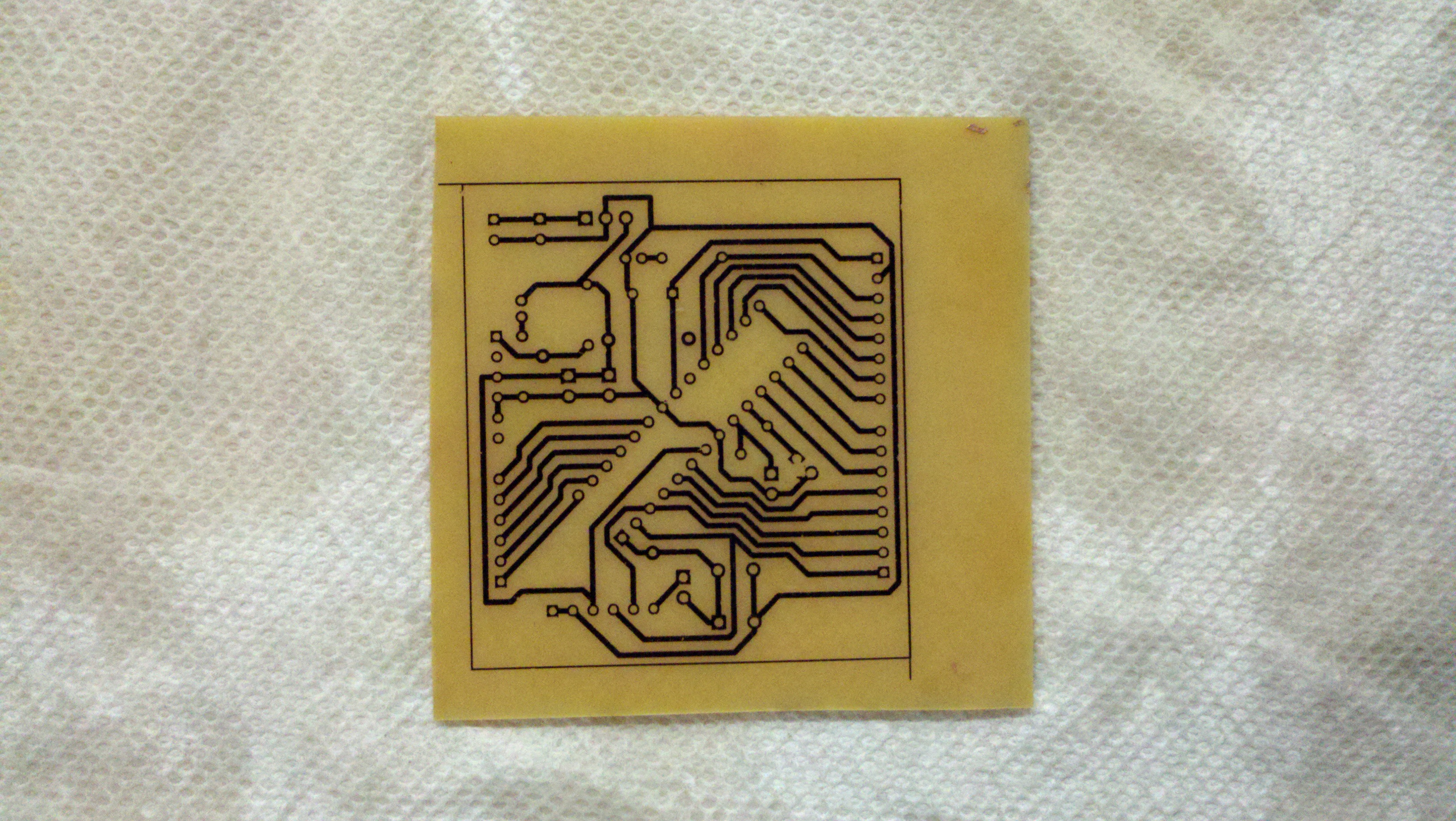
Etched top toner removed
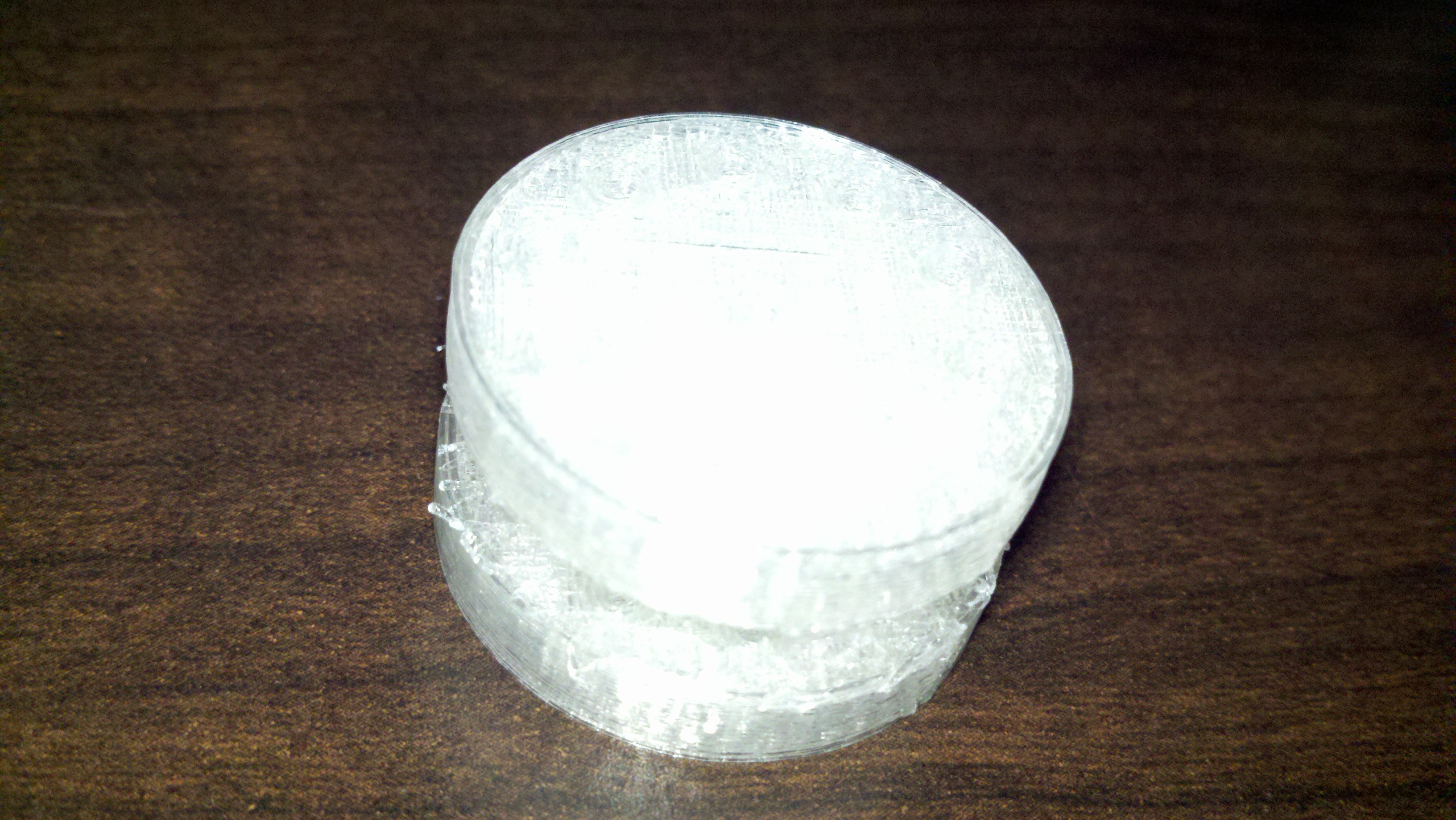
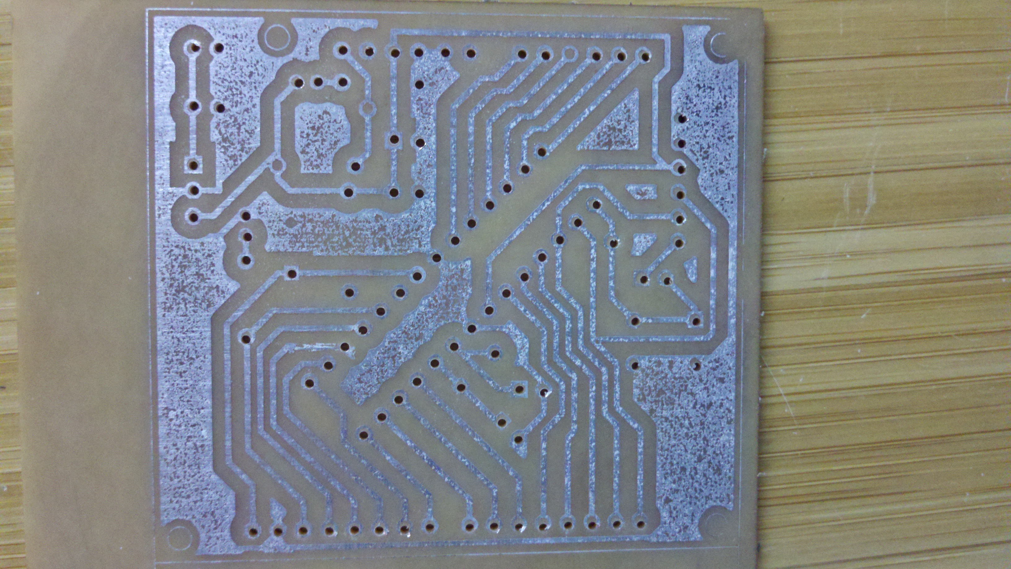
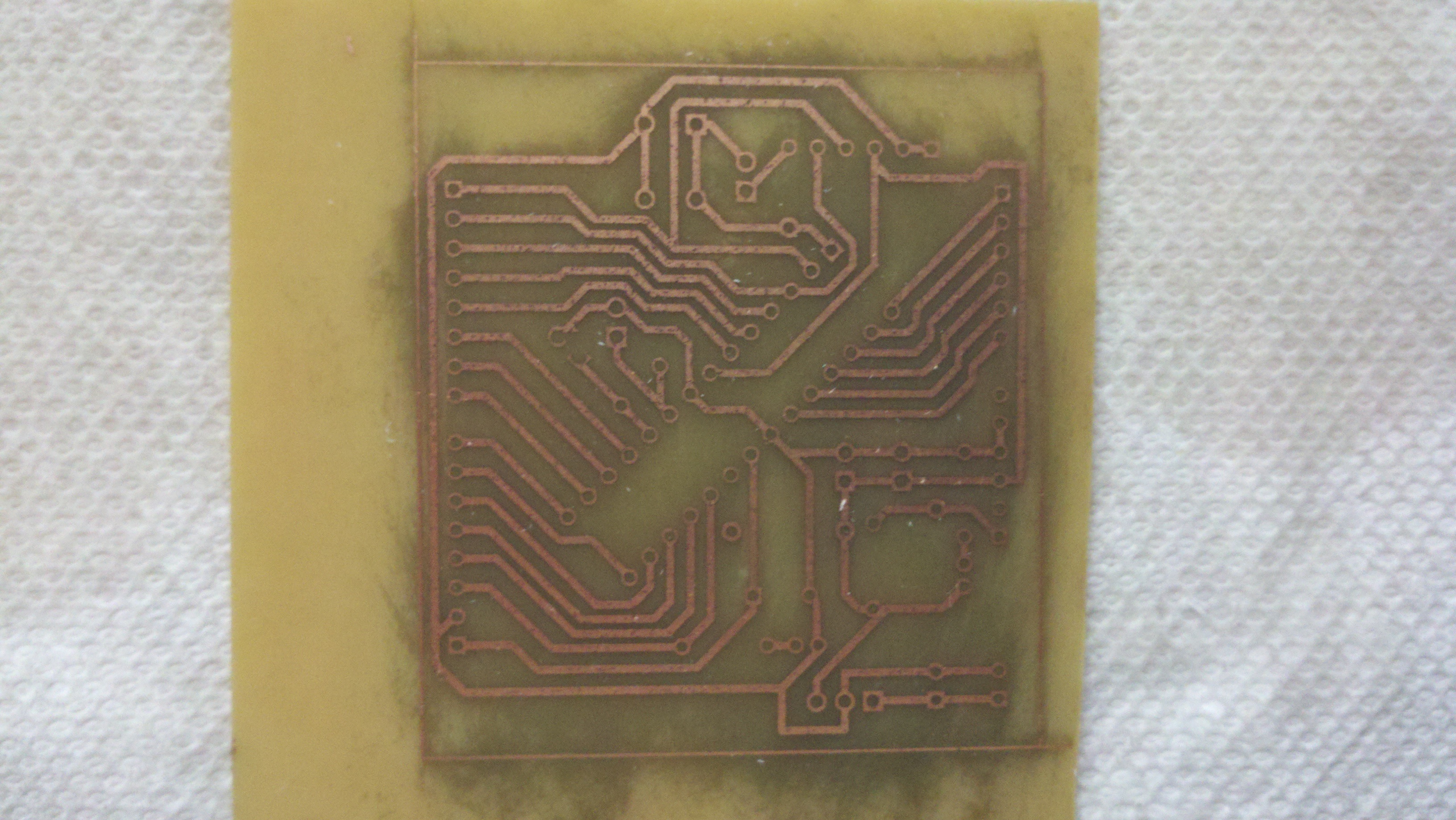
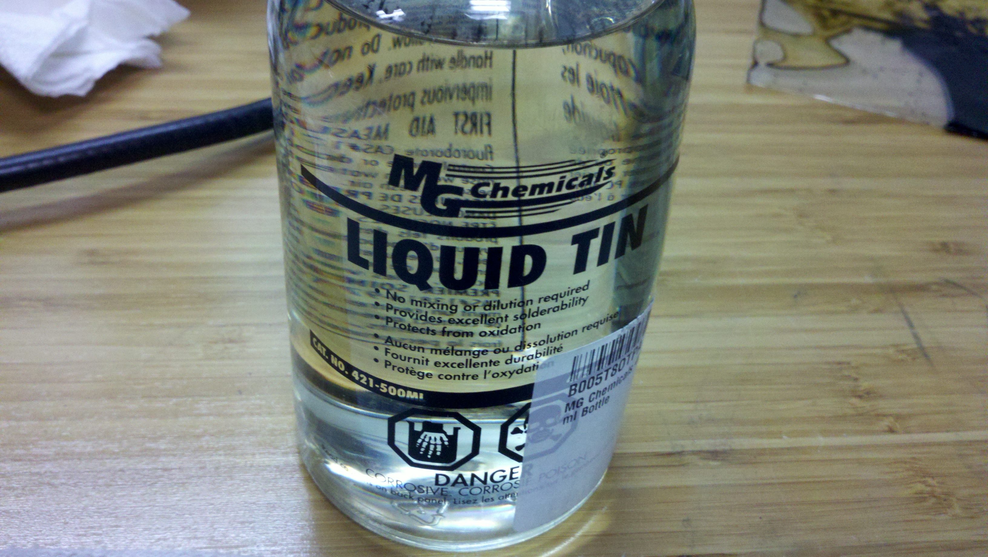
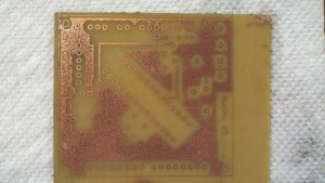
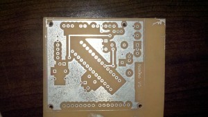
Bottom with tin

Top with tin

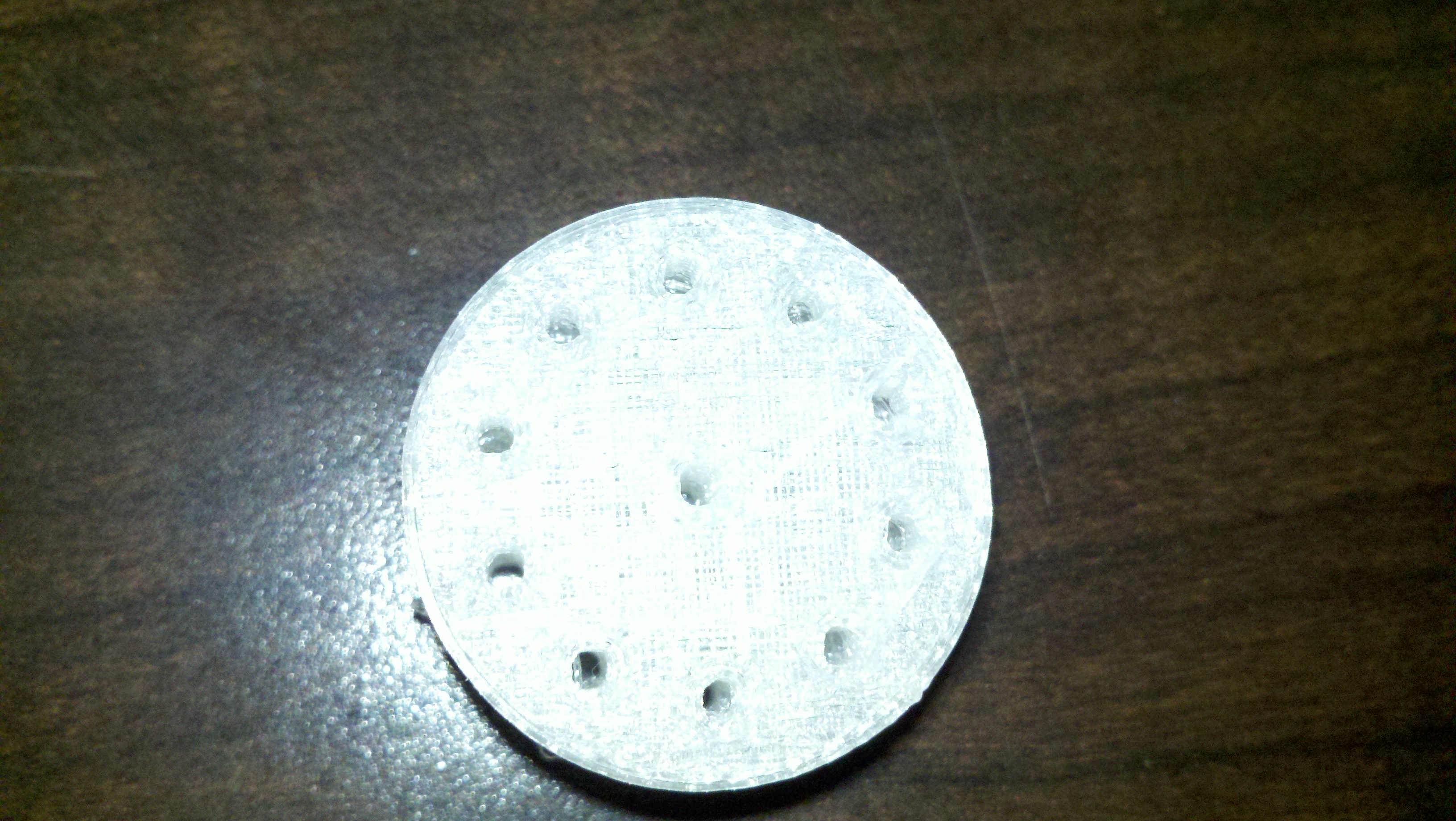
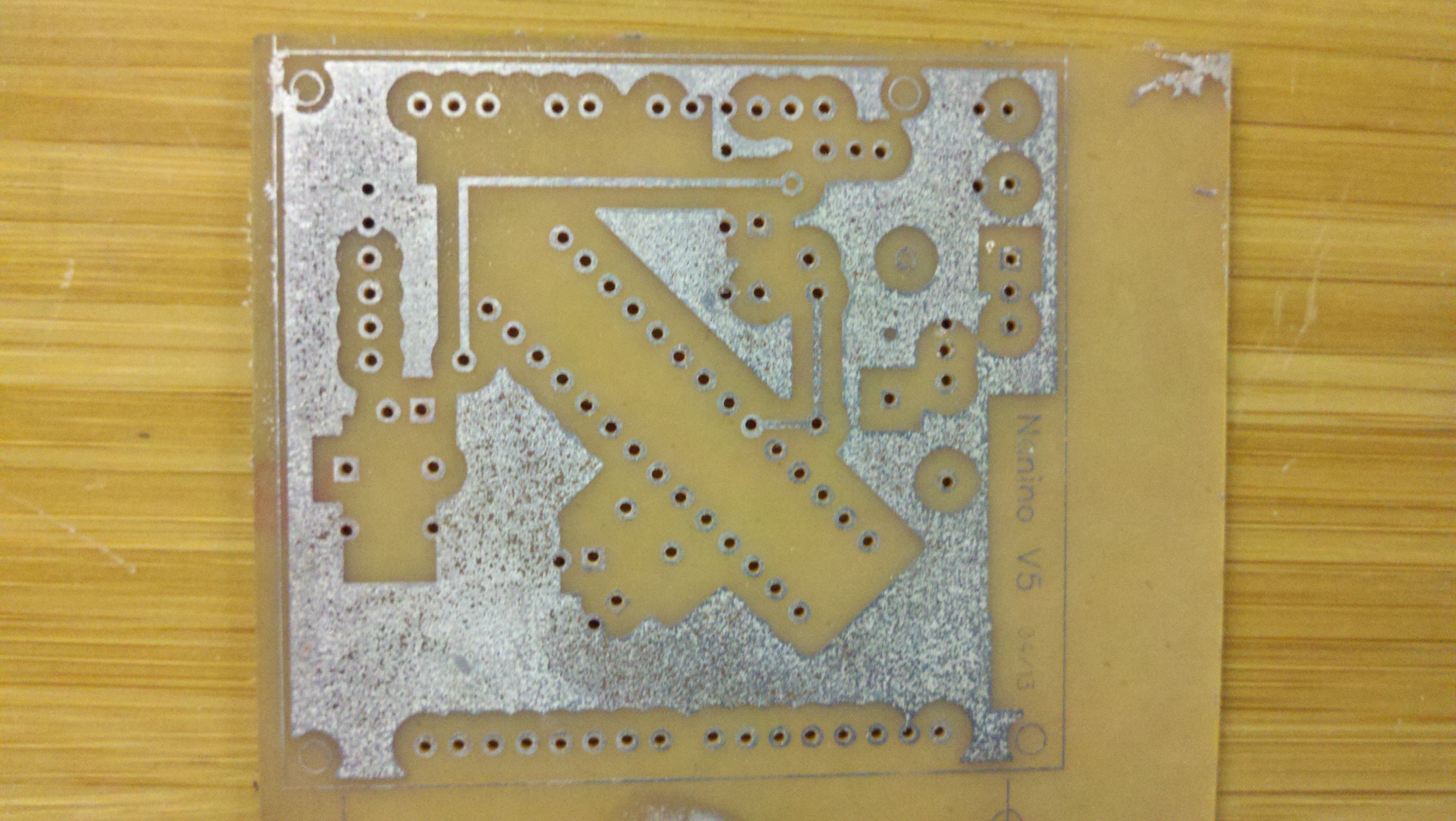
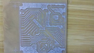
Top with holes drilled
Bottom with holes drilled
Another of top with mount holes
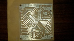
Another of bottom with mount holes
Final thoughts on the second attempt. First I should remember to read my lessons learned so I do not repeat the same mistakes. I also think that I am at the stage where the board is usable and I think I will solder components to this one. Its not to the point where I am entirely happy with the results but I think that I am not too far away. I am going to make at least one more of these boards for a friend and I am sure that that one will be the best one yet.