Filastruder KickStarter – Update 1

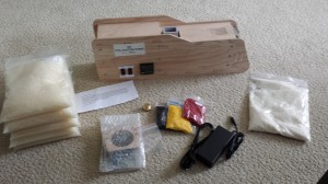
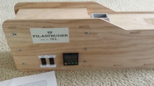
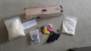
I backed a Kickstarter for the Filastruder  back in March and I finally received it.

20130626_181419 20130626_181434 20130626_181451

I have been busy since I received it so I have yet to test it.  That actually turned out to be a good thing.  I received an e-mail from the author saying there was a miss-wiring when they assembled it and it would need to be fixed.  I scraped together a bit of time this weekend and was able to repair the miss-wiring but I was not able to test the unit.  Couple other issues that I had are as follows:

  • I was able to fix the wiring as described by the e-mail from the author.  No issues
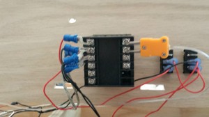
  • When I open the box I notice right away one of the leads to the thermocouple was disconnected.  I was able to reconnect it.20130630_145921
  • The leads on pin 2 also popped off due to the motor negative being extra short and me jostling it round (I decided to replace the lead to make it longer).  I was not able to put all three leads back to pin 2 on due to the connector ends taking up too much space.  I ended up soldering all but the heater line together so that I only had two connections to shove on to the terminal. A followup from the author said they are fixing the connectors to use better ones.
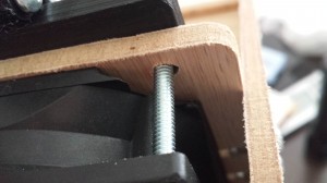
  • The 80 mm fan was damaged in shipping.  One of the corners broke off (the piece was not in the box).  The fan is still usable as only one side of the corner was damaged.  See picture.20130630_143314
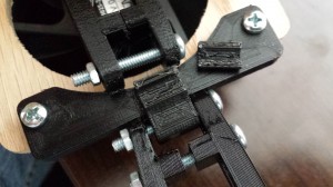
  • When putting the filament guide together the upper section of the 3D printed part that holds the vertical filament guide broke off.   See picture.  The author responded to my comments with a redesigned part that I will print as a replacement.20130630_143353

So far my impressions are good.  I like what they are doing and its encouraging that they are actively still working on it to resolve the problems.  This is after all a somewhat beta product and I would expect issues such as this.  So far the issues have been minor and have not prevented the use of the thing (only my lack of time).

I will post and update once I get some time to power the thing on and make some filament.  The prospects of this happening this week look bleak since the 4th of July is coming up.

PCB Etching – Update 5

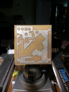
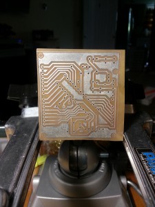
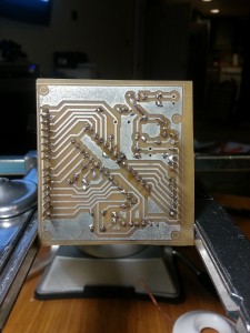
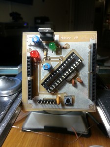
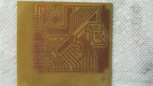
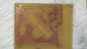
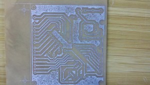
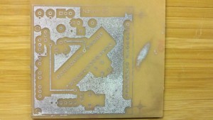
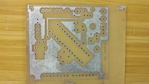
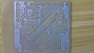
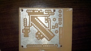
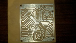
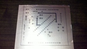
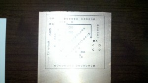
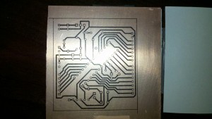
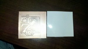
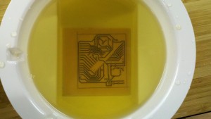
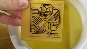
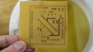
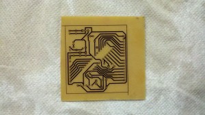
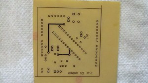
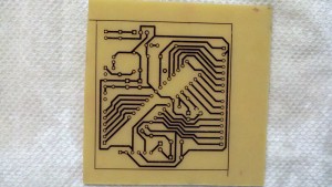
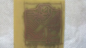
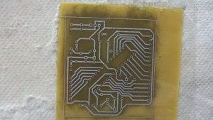
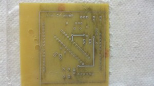
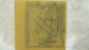
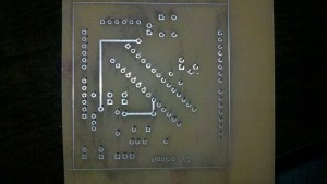
Another successful PCB Etch. As predicted this one is the best one yet. The top and bottom alignment is excellent, the traces are crisp and barely any pitting in the copper pours. I learned from the past and followed my own reminders of past mistakes and it came out great. Here are a few things we did different this time.

  • Open etch container. I was using a zip lock bag and      found that this did not work all that well. It did minimize the amount of      FeCl that is needed but it left bubbles on the board and did not have even      coverage. This time I used a wire and made a loop on both ends to hold the      board and dipped it in a shallow plastic container.
  • Since I was using a zip lock before I was placing the      whole zip lock with the board and FeCl in it into warm water to speed up      the etching. I was not able to do this this time with the open etch tank.      In the future it might be a good idea to figure out a way to heat the      liquid. It took about 30-35 mins of etching with unheated FeCl
  • I am still not exactly sure on how many passes it takes      through the laminator for a full transfer. I can say however that due to a      failed transfer 5 is not enough and 20 is enough.

Here are some pictures of the success:

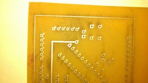
Top

Top

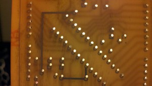
Bottom

Bottom

Bottom- Populated

Bottom- Populated

Top - Populated

Top – Populated

Centrifugal fan – Update 0

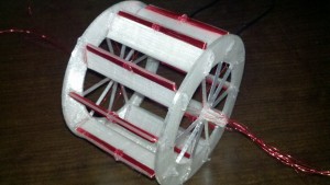
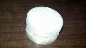
I have wanted to make an electric motor from scratch for quite a while now.  But instead of just making a motor and hooking it to something like a fan I had an idea.  What if the motor was integrated into the fan?  I tossed around some ideas putting coils on a propeller blade and got hung up on making the brushes and commentators.  I finally decided on doing a squirrel cage fan or if you want to get all scientifical a Centrifugal fan http://en.wikipedia.org/wiki/Centrifugal_fan.

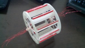
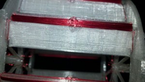
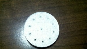
With a bit of magic (sure come call it 3D printing) here is the rotor/fan wheel assembled with 30 turns of magnet wire wrapped longitudinal around each one making a total of 10 coils.

assembled rotor

assembled rotor

assembled rotor

assembled rotor

Dab of hot glue to hold the coil in place

Dab of hot glue to hold the coil in place

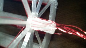
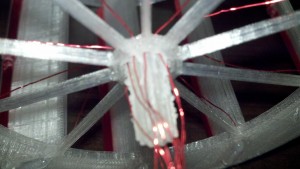
My plan for the commentators and brushes did not quite work out (this is prototyping after all) so I decided to redesign it and make it bigger and glue it on for now.  I will reprint it in one piece once I get the design squared away.

close up of failed commentator design

close up of failed commentator design

close up of failed commentator design

close up of failed commentator design

new design for commentator/ brushes design

new design for commentator/ brushes design

new design for commentator/ brushes design

new design for commentator/ brushes design

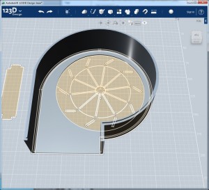
Moving on to the all-important housing which I am still designing.  I got the basic shape but I am still thinking about how to design the brushes mount and still print the thing in just two halves.  Here is the basic shape I am looking at more to follow once I finalize the design and print it out.

begining of housing design

begining of housing design

Nanino Share Alike

The original Nanino is licensed CC-BY-NC-SA, this one is also:
Creative Commons License
This work is licensed under a Creative Commons Attribution-NonCommercial-ShareAlike 3.0 Unsupported License.

Since I have now created one of these with success, I offer to the masses my modifications.  To summarize what I have done.

  • Original (where I got it from) http://www.meatandnetworking.com/projects/nanino-upgrade.  I actual original came from http://vonkonow.com/wordpress/2012/10/nanino-the-diy-friendly-arduino/
  • I added a 5v voltage regulator and supporting caps.
  • I added a 2 pin header for input on the unregulated side of the voltage regulator
  • I made the board two sided.  Previously the traces on the top were wires.  It will still work as a one sided board if you desire.
  • I added copper fills to the entire board.
  • Added registration marks for aligning the top an bottom
  • Added the name and version as a copper fill.  I used version number 5 arbitrarily for my own tracking purposes
  • Standardized all holes to size #65 for easy drilling
  • Increased all pad sizes to .075 for easy soldering and to resolve pad lifting issued when soldering

Please enjoy my modification and maintain CC-BY-NC-SA.  Thanks!

NaninoLVL1-mod5.1

PCB Etching – Update 4 IT’S ALIVE!!!

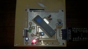
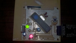
Success!!  Its a working Arduino!!!  I soldered all the components on the board.  It took me a bit to figure out which components are which since I do not have the silk layer and its slightly different from the original which has the values for the components.  I also have a few extra holes that I am not really sure what they are for.  I connected up my FTDI basic and uploaded good ol’ Blink and low and behold the GREEN FLASH OF GLORY!!!

Red led = life

Red led = life

Green flashy light

Green flashy light

2013-04-09_22-48-30_117

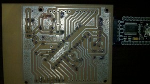
bottomI must note that the solder did not flow up to the top pads like a normal board with through hole plating.  This is not necessary on this board since it is mostly one-sided.  It does not have the mechanical holding on the components but I will try not to hang any weights from them.  I also did not solder all the headers on yet because I wanted to give it a try and it was getting late.  I will finish it up tomorrow.

PCB Etching – Update 3

I did another attempt at etching the same PCB from the previous posts.  I did a few things differently this time and got different results some good some bad.

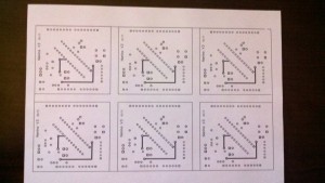
First I reworked the schematics.  I increased the pad size of all holes to .075.  When soldering some test legs to the previous etching I did we found that the pads detached from the board.  Hopefully the larger pad will prevent this.  Also I did a copper pour over the entire board to reduce the amount of etching that needs to take place.  I did this mostly to save on enchant but it also seem like a good idea.  Also as I found from the previous attempt that when printing on the transfer paper the top, which has the name of the board and version, should be mirrored when printed (instead of mirroring the bottom).  That way when it is transferred it will read correctly.  I also added registration marks to the print for aligning the top and bottom.

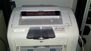
Second, a friend found a great deal on a HP Laserjet 1018 at a HAM fest for a whopping $5.  No really, just five whole dollars that is it.  Since we had problem printing on the paper we needed another printer and this one worked great.  It printed fine on the toner transfer paper and it transferred cleanly and completely.

2013-04-08_06-54-15_987

Third I modified slightly how I did the alignment of the top an bottom.  Unfortunately I forgot to take pics to help explain the process (I will try to do better next time).  Basically what I did was to take a scrap piece of PCB that is in an “L” shape. I took the top print (cut to approximate size) and taped it to the “L” scrap.  I next used the registration marks and center punched and drilled a hole through the board.  Next I used the holes to align the bottom print using the registration marks and shining a light through the paper.  I then slipped the PCB I was going to tech into the “pocket” and taped the prints to the board.  Finally I removed the scrap.  I realize that this is a bit difficult to explain an I promise that next time I will snaps some pics.  Ultimately the alignment is spot on and I am very happy with the results as you will see in the pics below.

So far so good, now what?  Well apparently I didn’t read my lessons learned from my previous attempts and I forgot to rinse the board after doing the transfer.  This made it take forever for the board to etch.  Even longer that before.  I ended up leaving the board in the solution for 45-50 mins.  This cause other problems it seems that the acid got through the toner an started to pit the copper pores.  It does not appear to have adversely effected the functionality of the board but, it does not look a nice as it should.  Also during the etching phase I learned another lesson.  I was placing the PCB in a zip lock with the ferric chloride and this tended to leave bubbles and places where there was little to no solution.  I do not think that I will use this technique again and instead just place it in a tub.

So without further adieu

Etched bottom toner removed

Etched bottom toner removed

Etched top toner removed

Etched top toner removed

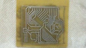
Bottom with tin

Bottom with tin

2013-04-07_18-23-16_868

Top with tin

Top with holes drilled

Top with holes drilled

Bottom with holes drilled

Bottom with holes drilled

Another of top with mount holes

Another of top with mount holes

Another of bottom with mount holes

Another of bottom with mount holes

Final thoughts on the second attempt.  First I should remember to read my lessons learned so I do not repeat the same mistakes.  I also think that I am at the stage where the board is usable and I think I will solder components to this one.  Its not to the point where I am entirely happy with the results but I think that I am not too far away.  I am going to make at least one more of these boards for a friend and I am sure that that one will be the best one yet.

PCB Etching – Update 2

Finally some success!!! I was able to successfully etch a PCB this weekend.  I followed many different tutorials (which you can find by asking Google) and this how I did it.

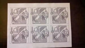
  1. Printing the schematic.
    1. I purchased Toner Transfer Paper http://www.amazon.com/Toner-Transfer-Electronic-Prototype-Sheets/dp/B00B0ZDXB2/ref=sr_1_1?ie=UTF8&qid=1364912557&sr=8-1&keywords=toner+transfer+paper
    2. I used DipTrace http://www.diptrace.com/ to print the schematic
    3. Several printers did NOT work.  I think that you may have to use a black and white printer only
      Top

      Top

      Bottom

      Bottom

  2. I got some copper clad board http://www.radioshack.com/product/index.jsp?productId=2102495.  And cut it to approximately the right size for the PCB that I was making. In the future I don’t think that I will cut the board until after I do the transfer.  This should reduce the waste board.
  3. I then thoroughly cleaned the board using acetone and paper towels making sure not to leave fingerprints on the board once cleaned
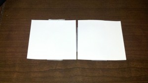
  4. Next I cut the schematics (top and bottom) and taped two sides together to make a “pocket” for the copper clad board. In retrospect this did not align the two sides correctly.  I think this technique will work but I need to use a spacer made from scrap pcb so that the alignment is correct (see picks below)
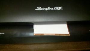
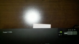
  5. I place the PCB into the pocket and ran the whole thing through a laminator http://www.amazon.com/Swingline-Fusion-Laminator-Warm-Up-1703074/dp/B009FFYIJA.  I didn’t really know how many times to run it through so I ran it through about 15 times. 2013-03-31_18-22-17_555 2013-03-31_18-22-27_109
  6. Surprisingly I did not have to soak the paper it simply lifted away and left the toner on the paper.  I am thoroughly impressed on the sharpness of the toner on the PCB.
    All the toner tranfered

    All the toner transfered

    2013-03-31_18-25-59_873 2013-03-31_18-25-50_886 2013-03-31_18-25-14_837 2013-03-31_18-25-07_267

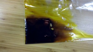
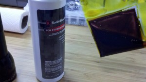
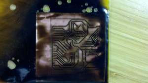
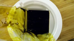
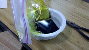
  7. Next I placed the PCB into a zip lock bag and poured in some ferric chloride http://www.radioshack.com/product/index.jsp?productId=2102868. I then place the zip lock into a tub of hot (from the tap) water.  This took longer than I expected.  I estimate that it took about 30-35 mins.  Although I did remove the board twice and rinsed it to check the progress. 2013-03-31_18-31-38_855 2013-03-31_18-31-51_657 2013-03-31_18-32-51_820 2013-03-31_18-41-35_988 2013-03-31_18-41-42_307
  8. Once it was fully etched I remove it an rinsed it in water and dried it with paper towel. 2013-03-31_19-10-49_875 2013-03-31_19-10-59_557 2013-03-31_19-11-09_585 2013-03-31_19-12-24_765 2013-03-31_19-12-32_980 2013-03-31_19-12-40_876
  9. Next I used Acetone to remove the toner which is the black stains you now see. 2013-03-31_19-19-12_22
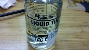
  10. Then I placed the PCB into another zip lock and poured in some Liquid Tin http://www.amazon.com/dp/B005T8PE4A/ref=biss_dp_t_asn.  This only took about 3 mins. And when it was done I rinsed in water again.  I also carefully poured the tin solution back into the bottle when I was done to reuse it later. 2013-03-31_19-19-35_114 2013-03-31_19-21-36_652 2013-03-31_19-21-45_527 2013-03-31_19-26-16_236 2013-03-31_19-26-27_285
  11. Finally I used a Dremel Drill Press http://www.amazon.com/Dremel-220-01-Rotary-Tool-Station/dp/B00068P48O/ref=sr_1_1?ie=UTF8&qid=1364914163&sr=8-1&keywords=dremel+drill+press and a #65 (.035) http://www.amazon.com/gp/product/B000TY190C/ref=oh_details_o00_s01_i00?ie=UTF8&psc=1  drill to dill all the holes.   Used http://www.amazon.com/gp/product/B0000DD2N3/ref=oh_details_o00_s01_i03?ie=UTF8&psc=1 also to hold the tiny drill. 2013-03-31_20-02-11_496 2013-03-31_20-02-34_395  2013-03-31_20-03-06_90

This was the first time I did this so I do have some lessons learned:

  • When I printed the schematic I mirrored the bottom side of the PCB.  This is necessary to match the top and bottom.  The problem is that put the name of the board and date on the top of the board (copper pour).  This made the words mirrored.  If I had mirrored the top and not the bottom the words would have been correct.  I will do this in the future.
  • The top and bottom alignment we off significantly.  This is apparently the hardest thing in the whole process to do.  I think I will try using a spacer out of scrap PCB when I make the pocket.  If this does not work I may consider drilling a hole or two to match the top and bottom.
    Close up of misalignment

    Close up of misalignment

    Close up of misalignment

    Close up of misalignment

Final thoughts:

Ultimately I had fun doing this which was the whole point.  This was a bit more challenging that I had previously though (as my previous posts indicated) and I learned quite a lot.  I will not use this first board since the top and bottom alignment is off but, I will etch another just like it (with improvements) and assemble it.  I have passed along this board to a friend and he is going to try soldering legs to it to see how it behaves.

Free Sample – Ti SimpleLink Wi-Fi CC3000

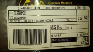
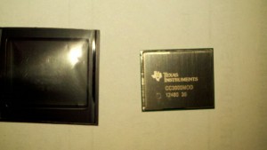
On occasion I sign up for free samples when the some of the sites I follow (http://hackaday.com/, http://dangerousprototypes.com ) report on them.  And on occasion I actually receive them.  This time I got a sample of the Ti SimpleLink Wi-Fi CC3000 http://www.ti.com/product/cc3000.

The TI CC3000 module is a self-contained wireless network processor that simplifies the implementation of Internet connectivity. TI’s SimpleLink Wi-Fi solution minimizes the software requirements of the host microcontroller (MCU) and is thus the ideal solution for embedded applications using any low-cost and low-power MCU (ref. http://www.ti.com/product/cc3000)

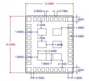
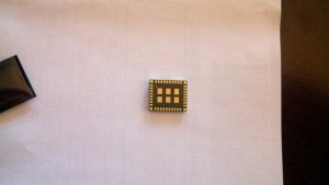
The module does have a somewhat difficult footprint to work with for a non-professional:

cc3000 footprint

cc3000 footprint

But they have posted schematics for a eval board design.  Hopefully I can take this and modify it to something that I can etch myself or possibly even get professionally done.  There seems to be some great resources on the Ti wiki http://processors.wiki.ti.com/index.php/CC3000.  At $10 per unit (at 1ku) I do not think it will be long before we see lots of these available for all sorts of hacker projects considering adding Wi-Fi to a project still costs $30-50.

2013-03-29_07-08-22_469 2013-03-29_07-08-41_537 2013-03-29_07-09-33_719 2013-03-29_07-10-02_554

PCB Etching – Update 1

Two posts in one night… man when it rains it pours I guess…

I had another update on the PCB etching.  Once again we failed.  This time I ordered some Toner Transfer Paper http://www.amazon.com/Toner-Transfer-Electronic-Prototype-Sheets/dp/B00B0ZDXB2/ref=sr_1_1?ie=UTF8&qid=1363659597&sr=8-1&keywords=toner+transfer+paper.  The failure was not with the paper though.  My friend tried to print the schematic onto the paper and the toner would not stick.  Most of the toner came right off.  Frustrated I call another friend with a laser printer to try his and it was slightly better but still terrible.  Finally I took the output pdf to work and printed there and finally success.

The only thing that I can think is that both printers that failed were color laser printers.  The first was a konica minolta 2500 and the other was as xerox 7500 ??? (Ill get the exact number soon).  The one at work was not a color laser just good ol b&w Xerox Phaser 3600 http://www.support.xerox.com/support/phaser-3600/support/enus.html?operatingSystem=winxp&fileLanguage=en.  The jury is still out on why the toner would not stick more investigation is required I guess.

Here is the schematic printed on the TTP ready from transfer.  Attempt number 3 will be coming soon.

Bottom

Bottom

Top

Top

3D Printed Case for the TrH Meter – Update 1

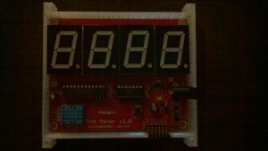
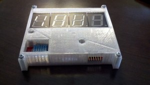
I am happy to report success with creating a 3D Printed Case for the TrH Meter from previous posts.  This is the first 3D object that I made from scratch!  I published it on the Thingiverse http://www.thingiverse.com/thing:62990.  I must say that once I watched the Ben Heckendorn video the design became really easy.  I highly recommend the video http://i.materialise.com/blog/entry/tips-and-tricks-by-ben-heck-how-to-use-autodesk-123d-design if you want to do a box similar.  My total design time was about 4 hours and the print took 2 hours (top and bottom).

I did also design another case/box for a friends electronics project (maybe another post on that one too) and that only took about 2hrs.  I suspect the next one will be even faster.

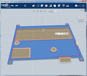
Here is a screenshot of my base.  This is all the dimensions of all the features of the box.  Think of this as a 3D object that is squished and flattened into a 2D object.  Make sure that you save this off because you will need it again for the bottom.  If you find you need to make changes it’s a good idea to save off back to the base so that you are working off the same file for the top and bottom.
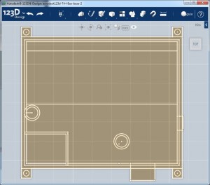
2DBase

The drawing is relatively easy to do using the Sketch (2D) menu.  This is just a series of squares lines and circles

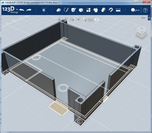
For clarity I thought I would point out some of the features of this base.  There is an “air” space between the PCB and the walls of the box I have highlighted them here:
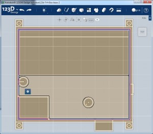
AirSpaceBorder

Highlighted here are the outer wall that will extruded up to make the sides of the box
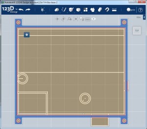
OuterEdges

The holes in the middle are for the reset button and for the light sensor.  The 7 seg displays will dim when it’s dark so you are not blinded by them.

Step two is to start the extrusion.  You need to extrude common components together.  This does take a bit of thought since you can only extrude a part once (which is no big deal).

Here I am extruding the underside of the PCB
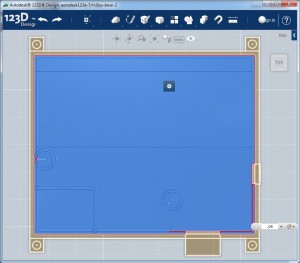
BottomExtrude-1

And here is the result.  It’s difficult to see but this is a 3D of the base that is .05 inch tall
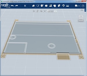
BottomExtrude-1a

The next step is extruding the sides of the box.  Notice that I do NOT have select two pieces on the side as those are the bottom part of the holes for the power and serial connection which I want to be a different height.
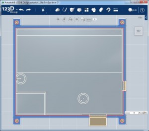
BottomExtrude-2

Now it’s starting to look like a box

BottomExtrude-2b

And finally with the pieces under the holes extruded.
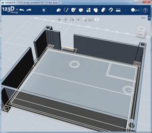
BottomExtrude-3a

We can we can send this to the printer by selecting everything and exporting it to .stl.  And while that’s printing we can move on to the top.

Start again from the base, this time we are going to extrude in the negative (-) direction.  Essentially extruding down towards the bottom (which extruded up towards the top).
Here is a shot of my first print where I forgot to extrude down.  You can see that the protrusions are sticking up from the box.  Oops.
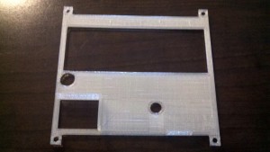
oops extruded in the wrong direction

Here is first extrude

TopExtrude-1

Next is a small area that encloses off the temperature and humidity sensor from the other components and leaves it open to the front from measurement. Remember when entering the extrude dimension to add the first extrusion to the distance you actually want it to protrude.  For example my top most piece is .05 inc thick and I want the protrusion to stick down .5 inch you need to extrude to .505 to get the correct depth.
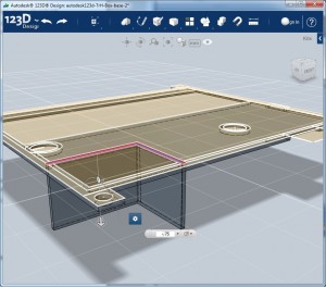
TopExtrude-2

Next I extrude the holes that surround the reset button and the light sensor (that dims the 7 seg displays when it’s dark)
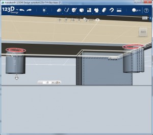
TopExtrude-3

Then finally the top part of the hole to make the serial connection just a small sliver of a hole on the side of the box.
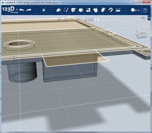
TopExtrude-4

Now we need to move the thing back to the ground plane.  To do this select the whole thing and click move.  Grab the up arrow on the movement directional and drag up. This will allow you to type the number in.  This number is the maximum amount you extruded into the negative.  In my case it was .505.
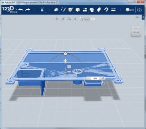
TopMoveUp

Then we need to rotate the thing 180deg for printing.  Select the whole thing again and click move.  This time grab the circle above the up arrow and rotate it.  Again the box will appear to allow you to type 180 deg.
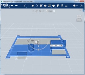
TopRotate

Sweet! Hopefully by now the bottom is done printing (mine took 1h 23 min).  Peal that thing off and send the top to the printer.

Here is the correctly printed top
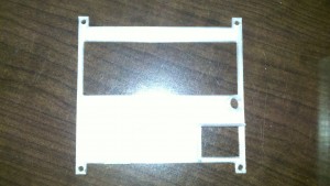
2013-03-17_17-53-48_975

And here is bonus mistake again on the top.  I forgot to leave out the hole above the humidity sensor.
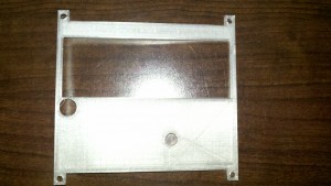
oops 2

The top printed in 37 mins.

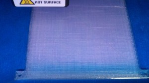
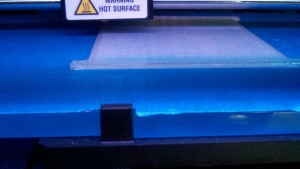
Here are some pick of it printing and the final product.  Don’t forget to post it out on the Thingiverse.
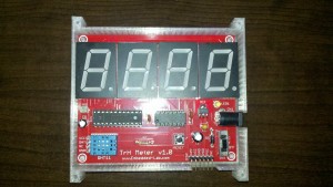
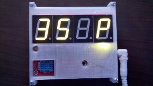
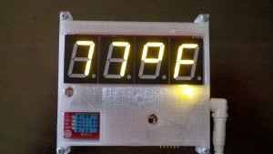
2013-03-17_17-53-32_209 2013-03-17_17-53-23_218 2013-03-17_17-52-01_901 2013-03-17_17-51-43_996 2013-03-17_15-50-39_430 2013-03-16_12-18-06_163 2013-03-16_12-17-57_813 2013-03-16_12-17-47_856